|
 
|
Welcome to the MicroElectromagnetics
Device Group
Pardon the chips and cracks, we are under
"restoration"
On-going research and teaching performed under the supervision of Dr. Dean P. Neikirk,
Dept. of Electrical and Computer Engineering
last update:
11/11/13
|
|

Hey, one of our research projects even made Jay
Leno's monologue!!
The Microelectromagnetic Devices Group studies the electromagnetic behavior
of structures fabricated using integrated circuit processing techniques.
For instance, understanding high-speed digital signal propagation between
integrated circuits, IC packages, and high-performance printed wiring boards
requires a background in solid-state devices, IC fabrication, and electromagnetics.
Similarly, constructing new devices and circuits that operate at extremely
high frequencies requires the same background. A major Microelectromagnetic
Devices Group objective joins these diverse areas to explore high-speed and
high-frequency circuit and device behavior, through both models and experiment.
An exciting new area of research involves the development of new sensors
using microfabrication techniques. In some cases these sensors are analogs
of natural senses; for instance, we are working on an "electronic tongue"
for use in new
chemical and biological agent sensors. Another area of research
is the study of how biological
entities detect infrared radiation, and the application of this knowledge
to engineered IR detectors (such as microbolometers). We are also investigating
the use of simple, low cost wireless sensors for "structural
health monitoring" to identifying material degradation in large civil
structures (bridges and buildings) before actual failure of the structure. This work is all generally
related to the fabrication and design of new
micro-sensors and actuators using IC processing and silicon micromachining
(mems). These sensors include optically
interrogated pressure sensors using micromachined Fabry-Perot cavities,
and microminiature
inductive proximity sensors. We have also investigated the application
of MEMS technology in such novel environments as mechanical
bearings and fluid seals.
Another major emphasis of our group has been the development of models of
lossy transmission lines
and interconnects. We are particularly interested in the impact of finite
metal conductivity on interconnect characteristics, as well as the effect
of substrate conductivity (e.g., semiconductor
substrates) on signal propagation. Our models focus on the prediction
of inductive and resistive effects, from dc resistance and internal inductance
to skin-depth
and proximity effect-dominated behavior, in both the frequency and time
domains. We have done a variety of studies on planar inductors, including the
effect of semiconductor substrate
resistivity on inductor behavior.
Our group has done extensive work on monolithic microwave, millimeterwave,
and far infrared devices, in particular on planar
antennas, FIR detectors, microbolometers, high
frequency resonant tunneling diodes, and coplanar
waveguide phase shifters and delay lines.
Dr. Neikirk's group has also investigated devices based on quantum
interference effects. His group developed several quantum transport
models which were used to design heterostructure devices and, using the molecular
beam epitaxial crystal growth technique, these devices were fabricated. These devices
contained layers that are only a few atomic planes thick, causing very strong quantum interference. Originally these devices were
investigated for use as high
frequency oscillators, and were later studied for possible use as memory
devices.
The lighter side of science and engineering:
Ethical Behavior and Related Topics:
A total of  people have accessed this page since 1/19/96.
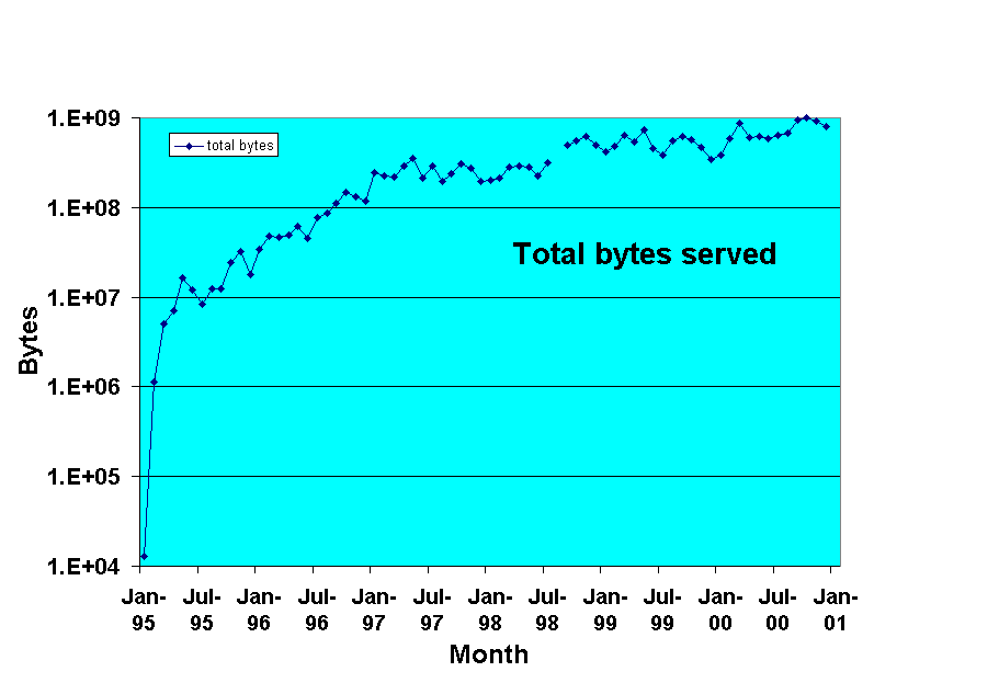
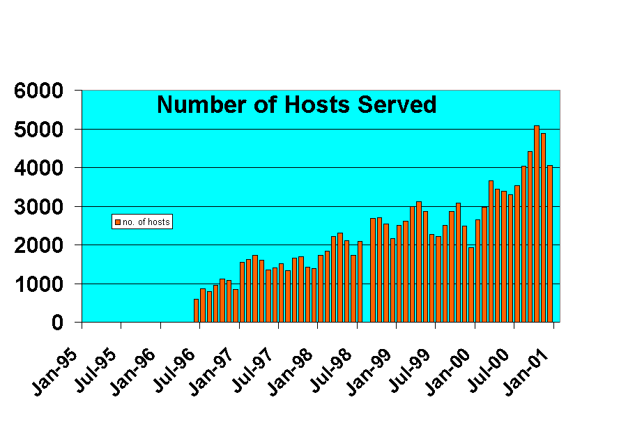
This page has been "on the air" since January
1995.
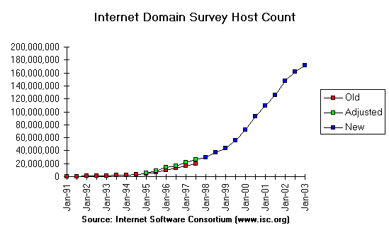
Source: Internet Software
Consortium ( http://www.isc.org/ )
Details on usage of this home page can be found by clicking
here.
If you have comments about this page, or would like further
information, please contact Professor Neikirk at
neikirk@mail.utexas.edu
This page was last updated on
November 11, 2013
.