Factors Affecting Microbolometer Responsivity
For a more complete discussion of this material, please see:
Jason Lewis, PhD Dissertaion: "Far-Infrared
and Sub-Millimeter Microbolometer Detectors," The University of
Texas at Austin, 1994.
Abstracted versions of some of our related publications and
talks available here on our Web site:
- Dean P. Neikirk, slides used in the talk "Micro-sensors
- what happens when you make "classical" devices "small":
integrated bolometric radiation detectors" (big file, about 700K)
- D. P. Neikirk, D. B. Rutledge, and W. Lam, "Far-Infrared
Microbolometer Detectors," Int. J. Infrared Millimeter Waves,
vol. 5, pp. 245-277, 1984.
- S.M.Wentworth, R.L. Rogers, J.G. Heston, and D.P. Neikirk, "Twin-slot multi-layer
substrate-supported antennas and detectors for terahertz imaging,"
First International Symposium on Space Terahertz Technology, University
of Michigan, Ann Arbor, Mich., March 5-6, 1990, pp. 201-213.
- J. M. Lewis, D. P. Neikirk, and S. M. Wentworth, "Low
growth temperature GaAs microbolometers," 15th International
Conference on Infrared and Millimeter Waves, R. J. Temkin ed., Dec.
10-14, 1990, pp. 398-400.
- S. M. Wentworth and D. P. Neikirk, "A
Transition Edge Microbolometer (TREMBOL) for Far-Infrared Detection,"
SPIE Conference on Superconductivity Applications for Infrared and Microwave
Devices, Orlando, FL, 1990.
2.2.1 Microbolometer Responsivity
One key figure of merit to consider when designing and optimizing microbolometer
performance is responsivity (r), since the signal voltages can be
quite low for these devices. A typical bismuth microbolometer has a responsivity
of about 20 volts/watt, and noise equivalent power (NEP) on the order of
 . The minimum detectable power will produce a signal
in the nano-volt to micro-volt range for measurements taken in the 1-1000
Hz range. Detectors with higher responsivities could ease the amplification
requirements in receiver systems by making it easier to detect these small
signals. The thrust of the modeling presented here will be toward maximizing
the responsivity of antenna-coupled microbolometers.
. The minimum detectable power will produce a signal
in the nano-volt to micro-volt range for measurements taken in the 1-1000
Hz range. Detectors with higher responsivities could ease the amplification
requirements in receiver systems by making it easier to detect these small
signals. The thrust of the modeling presented here will be toward maximizing
the responsivity of antenna-coupled microbolometers.
The signal voltage for a microbolometer can be related to the incident power
by using a simple circuit expression for responsivity, given by
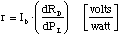 (2.14)
where Ib is the dc bias current through the detector,
and  is the change in resistance of the detector due
power absorption in the load. For conventional bolometers, the load element
also acts as the detector. The subscripts allow this expression to also
describe composite microbolometer operation, where the load and the detector
are separate elements.
is the change in resistance of the detector due
power absorption in the load. For conventional bolometers, the load element
also acts as the detector. The subscripts allow this expression to also
describe composite microbolometer operation, where the load and the detector
are separate elements.
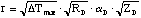
According to equation 2.14, the responsivity can be optimized by maximizing
the product of Ib and  . By breaking
these terms into physical constants, the role of the material properties
becomes much clearer. This relationship with physical properties is dependent
on the limiting mechanism of operation. The maximum bias current, for instance,
is likely to be limited by one of four things: 1) Thermal Limits
of the detector due to I2R (joule) heating, 2) Current density
limits in order to avoid electromigration failure in the detector element,
or due to the critical superconducting current density in superconducting
materials; 3) Bias-induced electric field breakdown across either
the detector material or the dielectric between the detector and the load,
or 4) Instability of the detector.
. By breaking
these terms into physical constants, the role of the material properties
becomes much clearer. This relationship with physical properties is dependent
on the limiting mechanism of operation. The maximum bias current, for instance,
is likely to be limited by one of four things: 1) Thermal Limits
of the detector due to I2R (joule) heating, 2) Current density
limits in order to avoid electromigration failure in the detector element,
or due to the critical superconducting current density in superconducting
materials; 3) Bias-induced electric field breakdown across either
the detector material or the dielectric between the detector and the load,
or 4) Instability of the detector.
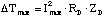
2.2.2 Thermally Limited Behavior
A microbolometer will experience heating due to the bias current as well
as from incident power. By far, most of the power will come from the bias
source across the detector. The maximum allowable temperature rise above
ambient ([Delta]Tmax)
 (2.15)
due to the maximum allowable dc bias power (Pmax) is
 (2.16)
where ZD is the thermal impedance of the detector, defined as
 (2.17)
Since the power dissipated in the detector is mostly due to joule heating
from the bias source, [Delta]Tmax can be represented as
 (2.18)
The maximum allowable detector bias current (Imax), in
terms of the maximum allowed temperature rise, is then
 (2.19)
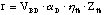
The second term in equation 2.14 can be broken down into the following physical
constants
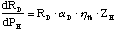 (2.20)
where aD is the temperature coefficient of resistivity
of the detector material
 (2.21)
[eta]h is defined as the thermal coupling efficiency between
the heater and the detector element
 (2.22)
and ZL is defined as the thermal impedance of the heater
element
 (2.23)
For a conventional bolometer, ZL = ZD,
and [eta]h = 1.
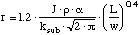
Substituting equations 2.19 and 2.20 into equation 2.14 reveals a new expression
which relates to the physical constants to microbolometer responsivity for
the thermally limited case.
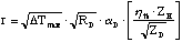 (2.24)
The bracketed terms are related, and cannot be varied independently. For
convention bolometers, this relation can be reduced to
 (2.25)
The relations in equations 2.24 and 2.25 can be useful in evaluating the
potential detector materials and configurations. The square root dependence
on [Delta]Tmax shows that the responsivity may be improved
by using detector materials that can withstand high temperatures. Materials
which are resistant to oxidation and melting would make good candidates.
Bismuth, because of its low melting point, is not capable of high temperature
operation. [Delta]Tmax could also be increased by lowering
the ambient temperature of the system. This is also likely to improve NEP
by reducing the thermally-induced component of noise. However, the thermal
conductivities of some materials, such as sapphire, increase with decreasing
temperature, resulting in lowered thermal impedances. For composite structures,
the dielectric layer must also be able to withstand operation at high temperatures.
Because [Delta]Tmax has only a square root dependence,
however, it is unlikely that this term alone would increase the responsivity
by more than a factor of two.
The relations above also indicate that an improvement in responsivity would
result from an increase in the thermal impedance of the detectors. It has
been shown experimentally that preventing the detector from contacting the
substrate by use of air-bridges increases the responsivity of a microbolometer
by increasing the thermal impedance of the detector [Neikirk, 1984 #1].
This method was reported to have increased responsivity by a factor of five,
and the sensitivity was improved by a factor of four. Choosing detector
materials to minimize thermal conductivity would also serve to increase
thermal impedances. This criterion would tend to favor semiconductor or
oxide materials over metallic detector materials. Choosing a high resistance
detector may also be an easy way to increase responsivity. Even though this
term has a square root dependence for the thermally limited case, it would
be easy to find a detector material with a resistivity of many orders of
magnitude higher than bismuth. For conventional microbolometers, the detector
resistance is fixed in order to be impedance matched to the antenna. For
composite structures, this restriction does not apply. The strong linear
dependence of aD on responsivity also makes this a key
parameter in detector material choice.
2.2.3 Current Density Limited
Another mechanism which may limit responsivity by limiting the driving current
through the detector may be device failure due to electromigration. The
current density may also be limited in the case of superconducting microbolometers.
In this case, it is assumed that the maximum allowable current is determined
by the maximum allowable current density through the detector element, rather
than a maximum allowable temperature rise. Although electromigration damage
is generally dependent on temperature in most systems, this analysis will
assume that the increase in temperature due to the bias current will be
small and thus have a negligible effect on the maximum current density.
Equation 2.26 shows an expression for responsivity that is algebraically
identical to equation 2.14.
 (2.26)
The maximum allowable current (Imax) can be related to
the maximum current density as
 (2.27)
where t is the detector thickness, and w is the detector width.
The detector resistance can be expressed as
 (2.28)
where [rho] is the resistivity of the detector material, and L
is the physical length of the detector. Substitution of equations 2.27 and
2.28 into 2.26, where Ib = Imax results
in the following expression for the dc voltage responsivity.
 (2.29)
For the case of the air-bridge bolometer [Neikirk, 1984 #1], the thermal
impedance will be independent of the detector length (see section 2.1.2).
For a given detector material, the length of the airbridge will determine
the maximum responsivity of the device.
For moderately long substrate supported microbolometers, the thermal impedance
is primarily determined by heat flow directly into the substrate. An empirical
approximation for this case was presented in section 2.1.3, and is shown
in equation 2.11. By using equation 2.11 to approximate Z, the responsivity
can be expressed as
 (2.30)
This equation will over estimate the responsivity for short detector lengths
due to the fringe mechanism of heat loss described in section 2.1.4.
These relations show that for bolometers in which bias current is limited
by current density, there is a linear dependence on [rho] as well
as a. This criteria would favor bismuth over other metals as a detector
material. Materials which are resistant to electromigration would also be
favored for this case.
2.2.4 Thermal vs. Current Density
Experiments have shown that typical bismuth microbolometers with the following
properties can be operated reliably for long periods of time at 2 milli-amps.
The devices become unreliable at around 3 to 5 milli-amps.
length |
4 um |
| width |
2 um |
| thickness |
1500 Å |
| resistance |
~ 100 [Omega] |
| responsivity |
~ 20 volts/watt |
| a |
~ 0.003 K-1 |
Table 2.4 Operating parameters for a typical bismuth microbolometer
For the dimensions listed in table 2.1, the current density at 0.003
amps would be 106 amps/cm2, which suggests the possibility
that failure may be due to electromigration damage.
The temperature rise due to the bias current can be approximated by using
 (2.31)
This estimates a 20 C temperature rise above ambient (~300 K) when biased
at about 0.003 amps. This temperature of ~45 C is much lower that the melting
point of bismuth (544 C), which makes it unlikely that failure is due to
melting of the bismuth element. Failure due to oxidation is also unlikely
if these temperatures are accurate.
Though the observations shown here are not entirely conclusive, they do
suggest that electromigration is the most likely mechanism for limiting
current in bismuth microbolometers.
2.2.5 Electric Field Breakdown
Composite microbolometers have an extra vulnerability that does not exist
with conventional microbolometers, in that voltage differences between the
heater and the detector element will result in high electric fields within
the dielectric that separates the two elements. The likelihood of accidentally
stressing the dielectric may be reduced by grounding one lead of the antenna
to one of the detector leads. The dielectric will also experience electric
fields due to the detector bias voltage. The electric circuit for electric
fields induced by the bias voltage is illustrated in figure 2.9. The highest
fields will be at E1, where they will be roughly
 (2.32)
where VD is the detector bias voltage, and tdie
is the thickness of the dielectric material that separates the heater from
the detector.
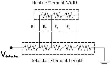
Figure 2.9 Electrical circuit for a composite microbolometer
showing the distribution of
electric field within the dielectric.
If electric field-induced breakdown is the limiting factor, then the
maximum responsivity can be given as
 (2.33)
where VBD is the breakdown voltage of the device.
This behavior would be more likely for high resistance detectors where high
bias voltages (> 10 V) could be used without dissipating much power.
For a dielectric thickness of 1000 Å, only 10 volts would be needed
to produce an electric field of 106 V/cm, which is about the
breakdown field of a good physically-deposited dielectric material. The
electric field through the dielectric could be reduced by using a thicker
dielectric, but at the expense of lowering the thermal coupling coefficient
([eta]h). Leakage currents through a stressed dielectric
may also contribute significantly to signal noise.
2.2.6 Microbolometer Stability
Another issue which affects microbolometer operation and can limit responsivity
is stability under constant bias conditions. Using a higher bias across
the detector will generally increase responsivity and thus will result in
a larger signal. A linear relationship between bias current and responsivity
is described in equation 2.14. and implies that it will be linear as long
as the other parameters (dR/dT, a, k) remain independent
of bias current.
It is important to remember that there are two components of power that
are dissipated in the detector. The incident radiation received from the
antenna is one component dissipated in the detector, and will be considered
an independent variable for this analysis. The other component is power
dissipated from the bias current, which will normally be much higher than
the incident power. The key point is that incident power (Pincident)
can influence the bias power (Pb) by changing the detector
resistance. This will result in either positive or negative feedback, depending
on whether the device is biased at constant current or constant voltage,
and whether the detector has a positive or negative temperature coefficient
of resistance.
Table 2.5 shows the conditions which result in positive or negative feedback.
Bias type |
Temp. Coeff. of Resistance |
Type of Feedback |
| constant current |
a > 0 |
positive |
| constant current |
a < 0 |
negative |
| constant voltage |
a > 0 |
negative |
| constant voltage |
a < 0 |
positive |
Table 2.5 Feedback bias relationships
For example, under constant current bias and a positive coefficient of resistance
(a > 0), incident power will increase the resistance of the detector.
Since the bias current is held constant, this will increase the bias power,
thus further increasing the resistance and further increasing the bias power.
Experience has shown that some operating conditions can result in unstable
positive feedback where runaway current destroys the device. Instabilities
even in large area (100 um x 1000 um) superconducting Bi-Sr-Ca-Cu-O bolometers
when operated at high currents have been reported [Lewis, 1989 #5], although
these devices were large enough to dissipate a 10 volt bias without destroying
themselves. Superconducting devices could be voltage biased in order to
avoid positive feedback; however, destructively high currents could occur
if the device temperature drifts too close to the superconducting state.
In these cases, the maximum bias conditions are lower than what would be
predicted when positive feedback effects are ignored. In order to better
understand and predict the maximum stable bias, an analysis is given here.
The following definitions will be used for this discussion:
r = small signal responsivity = 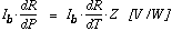
Ib = bias current [I]
Z = Thermal Impedance 
[Delta]Vn = Incremental feedback voltage across detector calculated
at nth iteration.
Po = Instantaneous Power at time = 0. (Bias + Incident. Does
not include feedback)
[Delta]Pn = Feedback power calculated at nth
iteration.
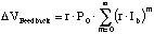
From the above definitions, [Delta]V1, the initial voltage
change across the detector due to the bias power and the incident power,
can be expressed as:
[Delta]V1 = r . Po (2.34)
The incremental increase in power dissipated in the detector (joule heating)
caused by the increased bias voltage can be expressed as:
[Delta]P1 = [Delta]V1 . Ib
= r . Po . Ib (2.35)
This increase in power in the detector then causes another incremental increase
in detector voltage that can be expressed as:
[Delta]V2 = r . [Delta]P1 = r .
Po . [r . Ib] (2.36)
Further iterations of the incremental increases in bias voltage due to feedback
can be expressed as:
[Delta]Vn = r . Po . [r . Ib]n-1
(2.37)
The total increase in detector voltage due to feedback can then be expressed
as:
 (2.38)
By using the following relation:
 for (A < 1) (2.39)
the total feedback voltage can then be expressed as
 (2.40)
From this relation it is apparent that the following must be true for stable
operation:
r . Ib < 1 (For stable operation) (2.41)
Another form of this relation looks like:

(2.42)
These results suggests that high resistance detectors would be more stable
than low resistance detectors. This criterion should be considered when
modeling low resistance detectors, such as superconducting microbolometers.
However, if high resistance detectors are integrated with a composite microbolometer
structure, operation may be limited by electric field breakdown in the dielectric
between the heater and the detector.
References
1. D. P. Neikirk, W. W. Lam, and D. B. Rutledge, "Far-Infrared Microbolometer
Detectors," International Journal of Infrared and Millimeter Waves,
5, 245 - 278 (3 1984).
2. S. M. Wentworth, "Far-Infrared Microbolometer Detectors", Doctoral
Dissertation, University of Texas at Austin, 1990
3. V. M. Abrosimov, B. N. Ergorov, and M. A. Krykin, "Size Effect of
Kinectic Coefficients in Poly Crystalline Bismuth Films," Sov. Phys.
JETP, 37, 113-116 (1 1973).
4. D. P. Neikirk, and D. B. Rutledge, "Air-bridge Microbolometer for
Far-infrared Detection," Appl. Phys. Lett., 44, 153-155 (15
January 1984).
5. J. M. Lewis, "Optical Detectors Based on Superconducting Bi-Sr-Ca-Cu-Oxide
Thin Films", Undergraduate Thesis, Massachusetts Institute of Technology,
1989