A total of people have accessed this page since 7/23/97.
This paper is abstracted from our original paper:
D. P. Neikirk, D. B. Rutledge, and W. Lam, "Far-Infrared Microbolometer
Detectors," International Journal of Infrared and Millimeter Waves,
vol. 5, pp. 245-277, 1984.
Also see the slide show on bolometers and infrared bolometric detection
of various sorts:
"Classical Devices Made
Small"
A great deal of effort is being applied to the development of monolithic
millimeter and submillimeter receivers. Because of the increasing loss and
mechanical complexity of metallic waveguide at these high frequencies, much
of this effort is devoted to quasi-optical Systems coupled to planar antennas
with integrated detectors [1][2][3]. These planar antennas have proved to
be quite different from their lower frequency counterparts [4][5][6]. The
integrated detectors have also presented real fabrication challenges. Planar
Schottky diodes, for example, will probably require submicron lithography
to avoid excessive parasitic capacitance at wavelengths less than one millimeter.
There is one antenna-coupled room temperature detector, however, that can
provide reasonably sensitive detection and speed without requiring elaborate
fabrication processes: the bismuth microbolometer.
Since the microbolometer is a thermal detector, it works well throughout
the far-infrared, without the capacitive roll-off that affects Schottky
diodes. It differs from more conventional thermal detectors, however, because
of its small size: typically four micrometers square and 100 nm thick. A
small device like this has a large thermal impedance, and so by using an
antenna to couple power into it large temperature rises can be achieved
(fig. 1). This in turn means the microbolometer will have a large responsivity.
In addition, since the thermal mass is also small, the detector can be quite
fast.
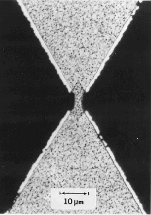
Figure 1: Top view of a typical antenna-fed microbolometer (to view a higher
resolution scan, just click on the image).
Two basic types of bolometers have been made: the air-bridge microbolometer
(fig. 2a) [7] and the more conventional substrate-supported bolometer (fig.
2b) [8]. A variation that takes advantage of the same thermal properties,
but avoids the necessity of biasing, is the bismuth-antimony micro-thermocouple
[9]. In this paper we will describe the thermal models that predict microbolometer
and microthermocouple performance, the restrictions placed on bolometer
materials for antenna-coupled detectors, the electrical measurements which
allow accurate detector calibration, and finally present results for a variety
of microbolometers we have made.
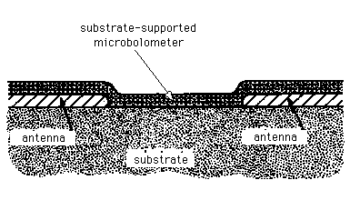
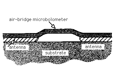
Figure 2: Cross sectional view of microbolometers; (a) air-bridge bolometer;
(b) substrate-supported bolometer.
The first microbolometers were substrate-supported devices. In these
bolometers the conduction of heat out of the detector into both the substrate
and the metal antenna are important. An exact solution to the thermal diffusion
equation is quite difficult since several interrelated conduction pathways
are available. The most obvious path is directly into the substrate material.
Another important source of heat loss is direct conduction into the antenna,
which is usually a metal with high electrical conductivity, and therefore
very high thermal conductivity. Less obvious, but probably important for
small detectors with large antennas, is conduction from the bolometer into
the substrate, and from there back into the metal antenna. Finally, if the
thermal conductivity of the bolometer material itself is small, this may
contribute significantly to heat retention in the bolometer.
The original work by Hwang et al. [8] used a considerably simplified but
physically helpful thermal model, which we follow here. In order to calculate
the conductance into the substrate the presence of the metal antenna is
ignored. The contact between bolometer and substrate is taken to be a hemisphere
of radius a, which is at a temperature ![]() . The thermal
diffusion equation giving the substrate temperature
. The thermal
diffusion equation giving the substrate temperature ![]() reduces to
reduces to
![]() (1)
(1)
which is solved subject to the boundary condition that ![]() for r
= a. Here KS is the substrate thermal conductivity,
for r
= a. Here KS is the substrate thermal conductivity, ![]() its density, and CS its specific heat. The solution
is
its density, and CS its specific heat. The solution
is
![]() (2)
(2)
where LS is the complex thermal diffusion length for the substrate,
![]() . The total substrate conductance is given by
. The total substrate conductance is given by
![]() (3)
(3)
which is here
![]() (4)
(4)
The total conductance G is taken to be this substrate conductance plus a
frequency independent contribution from the metal antenna, Gm.
The thermal impedance for the device is then
![]() (5)
(5)
where t is the bolometer thickness, w its width, and l its length; ![]() is the bolometer material density, and Cb its specific
heat. Finally, the responsivity of the detector is given by
is the bolometer material density, and Cb its specific
heat. Finally, the responsivity of the detector is given by
![]() (6)
(6)
where ![]() is the temperature coefficient of resistance of the
bolometer material, and Vb is the dc bias voltage across the
device. From eq. 5 we find
is the temperature coefficient of resistance of the
bolometer material, and Vb is the dc bias voltage across the
device. From eq. 5 we find
![]() (7)
(7)
where Gdc is the total dc conductance out of the bolometer, due
to both the substrate and metal contacts.
Hwang et al. [8] have also discussed the frequency response of this type
of microbolometer. For low frequencies when LS >> a (i.e. ![]() ), the thermal impedance is independent of frequency, and is given
by 1/Gdc. At higher frequencies when LS << a the
impedance varies like LS, that is f-1/2. At still
higher frequencies the thermal capacitance of the bolometer itself becomes
important, and Zt varies as f-1. Note also that both
the low frequency response and the speed of the detector increase as the
device size decreases. In contrast, as the substrate thermal conductivity
decreases the low frequency response increases, but the speed would be expected
to decrease.
), the thermal impedance is independent of frequency, and is given
by 1/Gdc. At higher frequencies when LS << a the
impedance varies like LS, that is f-1/2. At still
higher frequencies the thermal capacitance of the bolometer itself becomes
important, and Zt varies as f-1. Note also that both
the low frequency response and the speed of the detector increase as the
device size decreases. In contrast, as the substrate thermal conductivity
decreases the low frequency response increases, but the speed would be expected
to decrease.
A microbolometer's performance can be improved by increasing its thermal
impedance. The air-bridge bolometer does this by suspending the device in
the air above the substrate. The only conduction path is now out the ends
of the detector into the metal antenna. We can model this bolometer in a
particularly simple manner: a uniform bar of material in which power is
dissipated uniformly, and whose ends are attached to perfect heat sinks
(the metal of the antenna). The thermal diffusion equation describing the
temperature rise ![]() in the device is
in the device is
![]() (8)
(8)
where ![]() , Cb, t, w, and l are defined as before, Kb
is the bolometer material thermal conductivity, and Po is the
peak power dissipated in the bolometer. This equation is solved subject
to the boundary condition that
, Cb, t, w, and l are defined as before, Kb
is the bolometer material thermal conductivity, and Po is the
peak power dissipated in the bolometer. This equation is solved subject
to the boundary condition that ![]() is zero at the ends
of the detector. The solution is integrated over x to obtain the average
temperature rise in the device
is zero at the ends
of the detector. The solution is integrated over x to obtain the average
temperature rise in the device
![]() (9)
(9)
where Lb is the thermal diffusion length in the bolometer material,
![]() . The ratio of the time-varying temperature and time-varying
power yields the thermal impedance of the
. The ratio of the time-varying temperature and time-varying
power yields the thermal impedance of the
air-bridge bolometer,
![]() (10)
(10)
For the air-bridge bolometer, it is possible to plot a universal frequency
response curve (fig. 3). For low frequencies when the thermal diffusion
length Lb is much larger than the bolometer length l (i.e. ![]() ) the thermal impedance is independent of frequency, and
) the thermal impedance is independent of frequency, and ![]() . At high frequencies Lb becomes much smaller than l,
and
. At high frequencies Lb becomes much smaller than l,
and ![]() . These are the same limiting values as a thermal circuit
consisting of a resistance
. These are the same limiting values as a thermal circuit
consisting of a resistance ![]() in parallel with thermal
capacitance
in parallel with thermal
capacitance ![]() . Unlike the substrate-supported bolometers, the air-bridge
response changes quite abruptly from flat to a 1/f roll-off. The speed of
the detector is determined by (RtCt)-1 which is
. Unlike the substrate-supported bolometers, the air-bridge
response changes quite abruptly from flat to a 1/f roll-off. The speed of
the detector is determined by (RtCt)-1 which is ![]() . Note that the
speed depends on only one dimension of the bolometer, the length l . It
should also be noted that for fixed dimensions the thermal conductance out
of an air-bridge bolometer is always less than that out of a substrate-supported
device.
. Note that the
speed depends on only one dimension of the bolometer, the length l . It
should also be noted that for fixed dimensions the thermal conductance out
of an air-bridge bolometer is always less than that out of a substrate-supported
device.
The microbolometers discussed thus far measure the average temperature of
the entire device. We can also make a detector which measures the peak temperature
instead. This is done by using two different materials (for instance, bismuth
and antimony) to form a microthermocouple (fig. 4). We again assume the
silver antenna acts as a perfect heat sink, so the two ends of the device
are at the same temperature, To. The center of the detector where the contact
between the two materials is located is at a temperature To + ![]() . If the thermal-emf of the two materials are different there will
be an open circuit voltage across the junction
. If the thermal-emf of the two materials are different there will
be an open circuit voltage across the junction
![]() (11)
(11)
where a1 is the thermal-emf of one material and a2 the thermal-emf of the
other. The output signal then depends on the temperature difference between
the center of the device and the ends. From the solution to eq. 8 the ratio
Z of the time-varying temperature at the center of the air-bridge to the
power dissipated in the device is
![]() (12)
(12)
where Lb is again the thermal diffusion length, ![]() . The low frequency
limit is
. The low frequency
limit is ![]() , a factor of 1.5 larger than the low frequency average
thermal impedance Zt (eq. 10). The high frequency limit is the
same as before,
, a factor of 1.5 larger than the low frequency average
thermal impedance Zt (eq. 10). The high frequency limit is the
same as before, ![]() . Thus the peak temperature in the device
is described by a thermal equivalent circuit consisting of a resistance
. Thus the peak temperature in the device
is described by a thermal equivalent circuit consisting of a resistance
![]() in parallel with a capacitance
in parallel with a capacitance ![]() . The responsivity
of such a device is then found from eq. 11 to be
. The responsivity
of such a device is then found from eq. 11 to be
![]() (13)
(13)
Figure 4: Temperature profile in a microthermo-couple. The detector output
voltage is proportional to the peak temperature ![]() .
.
The choice of a material for use in a microbolometer is strongly dependent
on the electrical impedance desired. If we assume that the antenna is best
matched by a resistance Ra for a material with electrical conductivity
[[sigma]] we must have device dimensions that satisfy
![]() (14)
(14)
At the same time we want to maximize the thermal resistance to increase
the detector response. For an air-bridge bolometer we found that the thermal
resistance is proportional to ![]() , but using eq. 14 this is
just
, but using eq. 14 this is
just ![]() . Since Ra is fixed by the antenna we should
use a material which gives a large value for
. Since Ra is fixed by the antenna we should
use a material which gives a large value for ![]() .
.
The ratio of the electrical conductivity to the thermal conductivity, ![]() , is very nearly the same constant for most metals; the two properties
are fundamentally related. This relation is embodied in the Wiedemann-Franz
law, which gives
, is very nearly the same constant for most metals; the two properties
are fundamentally related. This relation is embodied in the Wiedemann-Franz
law, which gives
![]() (15)
(15)
where kB is Boltzmann's constant, e the electron charge, and
T the absolute temperature [10]. Because of this, for fixed device resistance,
almost all metals would give the same bolometer thermal resistance.
The other material constant that enters into the responsivity of the detector
is the temperature coefficient of resistance [[alpha]]; the larger [[alpha]]
the larger the responsivity. Once again, however, this is very nearly the
same for all metals because the resistivity [[rho]] near room temperature
is proportional to temperature. Using the definition of [[alpha]],
![]() (16)
(16)
we find that ![]() [11]. For 300 K this gives a temperature coefficient
of about 0.003K-1; almost every metallic element is within a
factor of two of this value.
[11]. For 300 K this gives a temperature coefficient
of about 0.003K-1; almost every metallic element is within a
factor of two of this value.
A search for materials with a large temperature coefficient usually leads
to a consideration of semiconducting materials. For intrinsic semiconductors
the carrier concentration varies exponentially with temperature, and their
resistivity is proportional to exp(E/2kBT). From eq. 16 this gives ![]() , where Eg is the band gap of the material. At room temperature
for a 1 eV band gap this is 0.06K-1, about twenty times larger
than that of a metal. Unfortunately this increase in a is more than offset
by a decrease in the material conductivity [[sigma]], since the quantity
we must really maximize is
, where Eg is the band gap of the material. At room temperature
for a 1 eV band gap this is 0.06K-1, about twenty times larger
than that of a metal. Unfortunately this increase in a is more than offset
by a decrease in the material conductivity [[sigma]], since the quantity
we must really maximize is ![]() . The conductivity in an
intrinsic semiconductor is usually 103 to 106 times
smaller than that of a typical metal, with a thermal conductivity 2 to 10
times smaller. This yields a figure of merit
. The conductivity in an
intrinsic semiconductor is usually 103 to 106 times
smaller than that of a typical metal, with a thermal conductivity 2 to 10
times smaller. This yields a figure of merit ![]() that is actually
smaller than a typical metal. If the semiconductor is doped to increase
its conductivity the resistivity is no longer proportional to exp(Eg/2kBT).
The carrier concentration is now set by the dopant concentration, and is
only weakly temperature dependent at room temperature. From fairly basic
considerations, then, a semiconducting material is unlikely to provide any
advantages as a microbolometer material.
that is actually
smaller than a typical metal. If the semiconductor is doped to increase
its conductivity the resistivity is no longer proportional to exp(Eg/2kBT).
The carrier concentration is now set by the dopant concentration, and is
only weakly temperature dependent at room temperature. From fairly basic
considerations, then, a semiconducting material is unlikely to provide any
advantages as a microbolometer material.
It would seem that almost any metallic material would make an equally good
bolometer. There is one practical constraint, however, that has not been
addressed. Generally the smaller the dimensions of a bolometer the better.
Using a photolithographic process capable of producing a minimum feature
size wmin the best microbolometer will be roughly wmin wide and wmin long
(i.e. one square). Since the desired resistance is Ra, we must
have a thickness that yields a resistance per square of Ra. There
is usually a minimum thickness, tmin, below which good deposited
layers are very difficult to produce, so the conductivity is constrained
by
![]() (17)
(17)
For a typical matching resistance of 100 Ohm and minimum thickness of 20nm
this gives [[sigma]] < 5x10³ (Ohm-cm)-1. In comparison,
the conductivity of copper is 6x10⁵ (Ohm-cm)-1, and
for lead is 4.8x10⁴ (Ohm-cm)-1. This constraint is
therefore quite serious, eliminating all the more common metals.
An examination of the elements shows very few with a conductivity low enough
to satisfy the restriction above. Since it is also advantageous to avoid
extremely large thicknesses (which increase the thermal mass and complicate
the fabrication process), we can also find a lower bound on [[sigma]]. Assuming
this maximum thickness to be 0.5um, the minimum conductivity is approximately
200 (Ohm-cm)-1. This eliminates several of the elements that
satisfied eq. 17. One material which does cover this range of conductivities
is thin-film bismuth.
The properties of thin-film bismuth are quite different from those of the
bulk material. Its conductivity is typically two to ten times lower than
the bulk, falling into the range desired for a microbolometer. The exact
value of its conductivity depends strongly on film thickness, substrate
material, and substrate temperature during deposition, and somewhat less
on evaporation rate [12][13][14][15][16]. The range of resistivities obtained
by different authors is fairly large, but under our deposition conditions
we have found our values of the resistivity to be repeatable.
Bismuth microbolometers have been made in several different ways. These
techniques fall into two general categories, the two-step process and the
single-step process. In a two-step process the antenna metalization is first
defined. The bolometer photoresist pattern is then aligned to the antenna,
the bismuth evaporated, and finally the lift-off performed. Single-step
processing uses a photoresist-bridge [17][18][19] or groove [20] so that
both the antenna and the bolometer can be formed with a single pattern in
one vacuum evaporation step.
Two-step processing has two major disadvantages. The first of these is technological:
for small antennas and small detectors the alignment between them becomes
very critical. The second is more fundamental: the low frequency 1/f-noise
in a two-step bolometer is usually significantly larger than in a single-step
detector. This is probably due to contamination of the first level metalization
during the second photolithographic step.
The photoresist-bridge technique has been widely used to fabricate a variety
of devices [21][22]. Figure 7 illustrates the general principle. In this
process the detector is formed under a bridge by evaporating bismuth at
an angle from both sides of the bridge. By evaporating different materials
from each side it is also possible to form bi-metallic junctions, such as
the bismuth-antimony microthermocouple (fig. 8) [9]. Note that this type
of process is self-registering; that is, the bolometer is aligned precisely
to the antenna since the same photoresist structure patterns both.
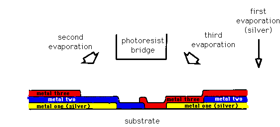
Figure 7: Photoresist bridge fabrication of bolometers.
The antenna metalization (silver) is evaporated at normal incidence, followed
by angle evaporation of the detector materials.
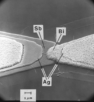
Figure 8: Bismuth-antimony microthermocouple. The SEM was taken at a 60o
angle to the substrate (to view a higher resolution scan, just click on
the image).
For substrate-supported detectors reductions in substrate thermal conductivity
offer a simple way to increase response. One possibility is the use of a
plastic to insulate the detector from the substrate. This approach has been
used in a 119um antenna array [23] that was fabricated on a silicon substrate.
Since silicon has a large thermal conductivity (about one hundred times
larger than fused quartz) bolometers made directly on it have very low responsivity.
By using a 0.5um thick layer of DuPont Pyralin 2555 (a polyimide) between
the microbolometer and silicon substrate a detector responsivity of 3V/W
at 0.1V bias was obtained. Comparable size devices on fused quartz gave
5V/W. From this we can see the excellent insulating properties of Pyralin,
with a thermal conductivity of only 0.15W(m K)-1 [24]. With this
in mind, we have fabricated substrate-supported bolometers both directly
on glass substrates, and with a 2um thick layer of Pyralin between the device
and the glass.
A somewhat more elaborate bridge process
is used to fabricate the air-bridge microbolometer. In the usual process
the bridge is suspended above the substrate by another layer of uniformly
exposed photoresist. This layer is then undercut during development to leave
the bridge above the substrate. In order to make the air-bridge bolometer
three layers of resist are used, with only the middle layer flood exposed.
Since we use transparent plasma-formed buffer layers [25][19] when the tri-layer
resist is contact printed to form the bridge pattern an identical pattern
is produced in the bottom layer. A finished photoresist structure is shown
in fig. 9. The antenna is formed by evaporating silver at normal incidence
to the substrate. Bismuth is then evaporated at a 500 angle from each side
of the bridge. The bolometer is thus formed under the bridge, but is supported
above the substrate by the bottom resist layer (fig. 10). After evaporation
the substrate is soaked in acetone for approximately one hour, which dissolves
all the photoresist. Unwanted metal on the top layer of resist is removed,
and the bolometer is left suspended by its ends above the substrate when
the resist below it dissolves away. A finished air-bridge detector is shown
in fig. 11.
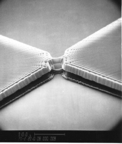
Figure 9: Photo-resist bridge pattern used to fabricate airbridge microbolometers
(to view a higher resolution scan, just click on the image).
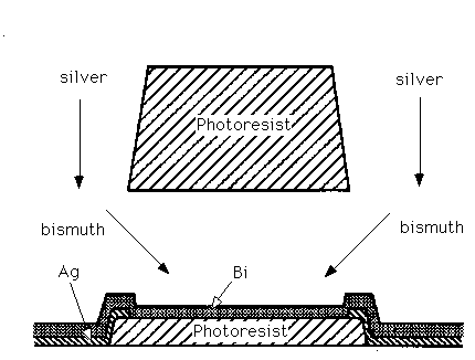
Figure 10: Evaporation sequence for air-bridge bolometers.
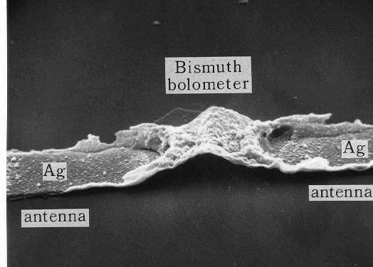
Figure 11: SEM of an air-bridge bolometer (to view a higher resolution scan,
just click on the image).
Unlike many far-infrared detectors it is possible to accurately calibrate
the bismuth microbolometer. This is done by first measuring the dc responsivity
of the bolometer from its dc I-V curve. An ideal bolometer has a resistance
R that is just a linear function of the power P dissipated in it,
![]() (18)
(18)
The low frequency voltage responsivity Rdc of such a device
with a constant bias current Ib applied to it is then
![]() (19)
(19)
We can find [[beta]] and Ro by measuring the dc I-V curve of
the bolometer, since eq. 18 gives
![]() (20)
(20)
Typical R-P plot for an airbridge bolometer produce linear regression fits
to the data with correlation coefficients usually better than 0.999. Note
that we can also find the dc thermal impedance Zdc of the device
once b is known using
![]() (21)
(21)
The NEP of a thermal detector has a fundamental limit, set by statistical
fluctuations in the power flow between the bolometer and its environment.
The mean square value ![]() of this fluctuation is given by
of this fluctuation is given by
![]() (24)
(24)
where G is the thermal conductance out of the bolometer and [[Delta]]f is
the detection bandwidth [26]. In terms of the complex thermal impedance
Zt this gives the minimum noise equivalent power as
![]() (25)
(25)
For the two thermal models discussed earlier Zt is independent
of frequency for low frequencies, so NEPmin is independent of frequency.
At high frequencies Re(1/Zt) varies like f1/2 so the
minimum NEP increases like f1/4. Note that the detector responsivity
decreases like f-1, so its actual NEP will increase as f, faster
than the fluctuation limit.
In conclusion, we have found the bismuth microbolometer to be a very useful detector. The simple fabrication techniques used make it quite easy to integrate into different antennas. Because it can be accurately calibrated it is useful in measuring the coupling efficiency of our antennas in conjunction with their quasi-optical systems. Finally, for wavelengths shorter than one millimeter, the microbolometer's sensitivity as a video detector is quite competitive with what can be obtained from other integrated detectors currently available.
[1] Clifton, B.J., G.D. Alley, R.A. Murphy, and I.H. Mroczkowski, 'High-performance
quasi-optical GaAs monolithic mixer at 110GHz,' IEEE Trans. Electron Devices
28, 155 (1981).
[2] Parrish, P.T., T.C.L.G. Sollner, R.H. Matthews, H.R. Fetterman, C.D.
Parker, P.E. Tannenwald, and A.G. Cardiasmenos, 'Printed dipole-Schottky
diode millimeter wave antenna array,' SPIE Proceedings Vol. 337, Millimeter
Wave Technology, May 6-7, 1982.
[3] Yao, C., S.E. Schwarz, and B.J. Blumenstock, 'Monolithic integration
of a dielectric millimeter-wave antenna and mixer diode: an embrionic millimeter-wave
IC,' IEEE Trans. Microwave Theory Tech. 30, 1241 (1982).
[4] Brewitt-Taylor, C.R., D.J. Gunton, and H.D. Rees, 'Planar antennas on
a dielectric surface,' Electron Lett. 17, 729 (1981).
[5] Engheta, N., C.H. Papas, and C. Elachi, 'Radiation patterns of interfacial
dipole antennas,' Radio Science 17, 1557 (1982).
[6] Rutledge, D.B., D.P. Neikirk, and D.P. Kasilingam, 'Integrated-Circuit
Antennas,' in
Infrared and Milliueter Waves, Vol. 10 (K.J. Button, ed.. Academic Press,
New York, 1983).
[7] D. P. Neikirk and D. B. Rutledge, "Air-Bridge Microbolometer for
Far-Infrared Detection," Applied Physics Letters, vol. 44, pp. 153-155,
1984.
[8] Hwang, T.-L., S.E. Schwarz, and D.B. Rutledge, 'Microbolometers for
infrared detection,' Appl. Phys. Lett. 34, 773 (1979).
[9] Neikirk, D.P., and D.B. Rutledge, 'Self-heated thermocouples for far-infrared
detection,' Appl. Phys. Lett. 41, 400 (1982).
[10] Ashcroft, N.W., and N.D. Mermin, Solid State Physics (Holt, Rinehart,
and Winston, New York, 1976), p. 255.
[11] Smith, R.A., F.E. Jones, and R.P. Chasmar, The Detection and Measurement
of Infrared Radiation (Oxford University Press, London, 1968), p 85.
[12] Colombani, A., and P. Huet, 'Electromagnetic properties of thin films
of bismuth,' International Conference on Structure and Properties of Thin
Films, Bolton Landing, N.Y., 1959, (C.A. Neugebauer, J.B. Newkirk, and D.A.
Vermilyea, eds., Wiley, New York, 1959).
[13] Komnik, Yu. F., E. Bukhshtab, Yu. Nikitin, and V. Andrievskii, 'Features
of temperature dependence of the resistance of thin bismuth films,' Zh.
Eksp. Teor. Fiz. 60, 669 (1971).
[14] Abrosimov, V., B. Egorov, and M. Krykin, 'Size effect of kinetic coefficients
in polycrystalline bismuth films,' Zh. Eksp. Teor.
Fiz. 64, 217 (1973).
[15] Kawazu, A., Y. Saito, H. Asahi, and G. Tominaga, 'Structure and electrical
properties of thin bismuth films,' Thin Solid Films 37, 261 (1976).
[16] Joglekar, A., R. Karekar, and K. Sathianandan, 'Electrical resistivity
of polycrystalline bismuth films,' J. Vac. Sci. Technol. 11, 528 (1974).
[17] Dolan, G., 'Offset masks for lift-off photoprocessing,' Appl. Phys.
Let., 31, 337 (1977).
[18] Dunkleberger, L., 'Stencil technique for the preparation of thin-film
Josephson devices,' J. Vac. Sci. Technol., 15, 88 (1978).
[19] Neikirk, D.P., 'Integrated detector arrays for high resolution far-infrared
imaging,' PhD thesis, California Institute of Technology, 1983.
[20] P.P. Tong, D.P. Neikirk, D.B. Rutledge, P.E. Young, W.A. Peebles, N.C.
Luhmann, Jr., "Imaging Polarimeter Arrays for Near-Millimeter Waves,"
IEEE Trans. Microwave Theory Tech. MTT-32, March 1984, pp. 507-512.
[21] Dolan, G.J., T.G. Phillips, and D.P. Woody, 'Low-noise 115-GHz mixing
in superconducting oxide-barrier tunnel junctions,' Appi. Phys. Lett. 34,
347 (1979).
[22] Danchi, W.C., F. Habbal, and M. Tinkham, 'ac Josephson effect in small
area superconducting tunnel junctions at 604GHz,' Appl. Phys. Lett. 41,
883 (1982).
[23] Neikirk, D.P., P.P. Tong, D.B. Rutledge, H. Park, and P.E. Young, 'Imaging
antenna array at 119um,' Appl. Phys. Lett. 41, 329 (1982).
[24] Du Pont Co., 'Pyralin: polyimide coatings for electronics,' Bulletin
PC-i.
[25] Dobkin, D.M., and B.D. Cantos, 'Plasma formation of buffer layers for
multilayer resist structures,' IEEE Electron Devices Lett. EDL-2, 222 (1981).
[26] Smith, R.A., F.E. Jones, and R.P. Chasmar, The Detection and Measurement
of Infrared Radiation (Oxford University Press, London, 1968), pp. 211-213.
[27] Jelks, E.C., R.M. Walser, R.W. Bene, and W.H. Neal II, 'Response of
thermal filaments in
V02 to laser-produced thermal perturbations,' Appl. Phys. Lett. 26, 355
(1975).