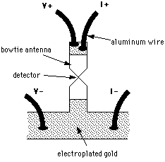
Fig. 1: The 4-point measurement setup for the Pb TREMBOL. Aluminum wire is thermosonically bonded to electroplated gold contact pads.
Stuart M. Wentworth and Dean P. Neikirk
Department of Electrical and Computer Engineering
The University of Texas at Austin
Austin, TX 78712 USA
ABSTRACT
Operation of detectors at low temperatures has the advantages of lower
noise and better thermal conditions. But detector responsivity for conventional
bolometers suffers from a drop in the temperature coefficient of resistivity
a as the temperature is lowered. The large a for a superconductor at its
transition between normal conductivity and superconductivity makes it an
ideal detector material for low temperature applications. However, it may
be difficult to control temperature to the center of such a narrow transition.
In this paper, the transition-edge microbolometer
(TREMBOL) is introduced. Following a brief background over superconducting
bolometers, a TREMBOL structure will be presented which uses the low transition
temperature (Tc) element lead as the superconductor. The paper
concludes with directions for future research.
2. BACKGROUND OF SUPERCONDUCTING BOLOMETERS
Both conventional and composite superconducting bolometers have been
fabricated. Conventional-type superconducting bolometers are large area
structures where the detector film also acts as the radiation absorber.
These have been built using tin[1]
and niobium nitride[2]. The first
bolometer to actually utilize the superconducting transition was a composite
structure using a blackened aluminum foil absorber in conjunction with a
tantalum temperature sensor[3]. Another
such composite structure makes use of aluminum as the temperature sensor
and bismuth as the absorber[4]. Recently,
an infrared detector which utilizes a weak-link mechanism rather than a
bolometric type mechanism has been fabricated using a bulk high transition
temperature superconductor (HTcS)[5]. Other works have focused on the use of superconductors for
optical and far-infrared detectors[6]
7-8.
The feasibility of a conventional-type bolometer using the transition of
a HTcS film has been discussed by Richards, et al. 9.
They obtained estimates of the sensitivity for such a bolometer by carefully
measuring the resistance and the low frequency noise in the transition region
of several HTcS samples. By assuming that sensitivity is not
limited by thermal conductance out of the device, a noise equivalent power
(NEP) as low as 10-12 W/was postulated.
Antenna-coupled microbolometers are faster and more sensitive than conventional
bolometers, and find use in imaging array applications. The idea of coupling
a superconducting microbolometer to a planar integrated antenna was first
suggested by Neikirk[10]. Such a structure
must perform three functions. It must absorb power from the antenna (i.e.
it must provide a matched load to the antenna impedance). It must
sense temperature changes due to the absorbed power (i.e. there must be
a thermal detector). And finally, it must bias the superconductor
to its transition temperature. If the ambient temperature is maintained
below the transition temperature, a heater can be used to provide
this bias. These three elements are not necessarily separate. In the simplest
configuration of the TREMBOL, for instance, the superconducting film would
act as both the load and the detector. In this case, the heater must be
separate, and most likely would control the overall temperature to bias
the entire array at the transition point. Such a TREMBOL is discussed in
section 3 using lead as the superconducting material. The feasibility of
a HTcS TREMBOL structure with an NEP possibly as low as 2.5 x
10-12 W/has recently been discussed by Hu and Richards[11].
A problem with this simplest configuration of the TREMBOL is that the superconducting
thin film resistivity throughout the transition region may be too low to
provide a matched load to the antenna. A 4 um x 4 um square of 1000 Å
thick YBCuO type superconducting thin film would have a transition region
resistance of no higher than about 20 [Omega]. Typical planar antennas,
on the other hand, generally have impedances in the 100-300 [Omega] range.
One structure which could possibly match to a HTcS resistor is
a twin slot antenna[12] which drives
the detector via a microstrip network. It is theoretically possible to achieve
imbedding impedances as low as 5 [Omega] with these slot antennas. Another
way to overcome the matched load problem is to build a composite TREMBOL
structure, which is discussed in section 4.
3. THE TREMBOL USING A CONVENTIONAL SUPERCONDUCTOR
To investigate the TREMBOL, a lead detector element coupled to a bow-tie
antenna was fabricated. Pb was chosen as the detector material because its
transition temperature is above the boiling point of liquid He, and because
it is easy to evaporate. Lead bismuthide devices were also attempted, but
PbBi forms a discontinuous film unless it is evaporated on a cold substrate
(on the order of 77 K). Pb is not without its own problems; our devices
oxidized and became useless after about 48 hours of exposure to air.
The Pb devices fabricated were 4.5 um long, 5.0 um wide, and 1000 Å
thick. Prior to device fabrication, gold contact pads were electroplated
on the glass substrate. The antenna metal was gold, and chrome was used
to promote adhesion. The Pb detector/Au antenna devices were fabricated
using a bilayer photoresist process which produces a narrow photoresist
bridge and a lip in the upper resist layer suitable for liftoff[13]. In this technique, metal for the antenna
is evaporated at normal incidence to the substrate, and the narrow photoresist
bridge casts a shadow in the detector region. The microbolometer material
is then evaporated at an angle to the substrate such that deposition is
accomplished under the photoresist bridge. The chip is soaked in acetone
to lift off the unwanted metal. Following liftoff, the chip was stored in
a desiccator to slow down oxidation of the Pb elements. Immediately prior
to testing, the devices were wire-bonded to the printed circuit board used
in the cryogenic testing apparatus. Aluminum wire was used, since it bonds
quite easily to electroplated gold. Figure 1 shows the placement of the
wire bonds to the tested TREMBOL. For maximum accuracy, a 4 point current-voltage
test is desired as close as possible to the superconducting element.
Preliminary evaluation of the TREMBOL requires a resistance plot across
the transition, and the resistance across the device as a function of power
dissipated in the element A bolometer characteristic is that its resistance
is a linear function of dissipated power. This property assumes that dR/dT
is constant over the temperature range considered, and that the temperature
change in the device is proportional to changes in its dissipated power.
This leads to an expression for dc responsivity (the response of a detector
to a step change in dissipated power)13,
rdc = Ib (dR/dP) . |
(1) |
|
Fig. 1: The 4-point measurement setup for the Pb TREMBOL. Aluminum wire is thermosonically bonded to electroplated gold contact pads. |
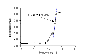
Fig. 2: The resistive transition for the 4.5 um long, 5.0 um wide, 1000 Å thick Pb TREMBOL. |
r = Ib R a |Zt| |
(2) |
Temperature (K) |
Bias current (mA) |
dR/dP (k[Omega]/W) |
Zth (K/mW) |
rdc (V/W) | |
| Pb: | 7.46 | - | - | - | - |
| 7.66 | 1.75 | 138 | 38 | 242 | |
| 7.75 | 1.0 | 274 | 76 | 274 | |
| Bi: | 300 | 1.0 | -20 | -67 | -20 |
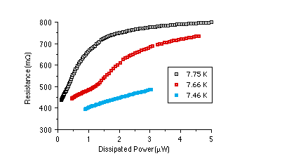 |
Fig. 3: Resistance-power plots at various temperatures near the transition for the Pb TREMBOL. |
4. COMPOSITE TREMBOL
One solution to the mismatched load problem is to separate the load from
the detector in a composite TREMBOL structure (Fig. 4). This type of device
follows from research using tellurium as the detecting element in a room-temperature
antenna-coupled composite microbolometer[14].
The load, which is matched to the antenna, may now also serve as the heater
by applying a dc bias through the antenna leads. The superconducting detector
element is in intimate thermal contact with, but is electrically isolated
from, the load/heater element. Changes in heater temperature will be quickly
followed by changes in detector temperature. As the detector changes temperature
in the transition region, large changes in resistance will occur, which
are measured with a current biasing circuit.
An advantage of this device is that the entire substrate can be cooled to
below the transition temperature, and the detector can be "turned on"
by applying a biasing current through the heater element. This can be quite
useful for multiplexing as discussed in section 4.1. The superconducting
film may also be used as a low-loss signal line away from the detector,
since the entire structure is cooled to below the transition temperature.
The device speed is limited by both the thermal mass of the heating element
and by the thermal conductance between the heater and the detector. The
detectable FIR frequency will be limited by the detector to load capacitance,
and therefore the overlap area must be kept small. For a 4 um x 4 um detector
separated from the load by 1000 Å of SiO2, capacitance
limits operation to below 100 GHz.
Fabrication of the composite TREMBOL involves a choice of superconducting
and resistive heater materials. The resistance of the heater material must
be known over the temperature range of interest, and the proper dimensions
must be chosen to achieve an impedance match with the antenna. Resistive
heater candidates include nichrome and bismuth. Superconducting materials
include the low Tc superconductors (such as tin, niobium, lead,
and lead bismuthide), and the new high transition temperature superconductors.
The HTcS materials, primarily YBaCuO compositions and related
compounds, were discovered by Bednorz and Müller[15], and improved upon by a host of researchers (see references
[16] and [17], and references contained therein). A variety of techniques
can be used to deposit thin films of these materials[18]-19[20].
One way to fabricate a composite TREMBOL would be to use a photoresist lift-off
technique for patterning the superconducting thin film. Following the deposition,
patterning, and high temperature anneal of this film, a thin (1000-2000
Å) layer of silicon nitride or silicon dioxide would be deposited
over the superconductor. This layer would serve as the electrical insulator,
but is thin enough to be a good thermal conductor. Finally, the antenna/heater
would be fabricated by the usual photoresist bridge technique used to make
bismuth microbolometers13.
Consideration must also be given to annealing and substrate effects, since
some of the more commonly cited substrate materials upon which superconducting
thin films are deposited (such as strontium titanate) are not particularly
good rf substrates. The more common substrates used in microwave circuits
have thus far produced inferior YBaCuO films; for

Fig. 4: Cross section and top view of a composite TREMBOL. Radiation is coupled into the load/heater by the planar antenna structure, causing a rise in the temperature of the load. Due to the intimate thermal contact between the load and the superconducting detector, the resistance of the TREMBOL changes. This resistance change is sensed by the signal line. |
4.1 Matrix addressing in a composite TREMBOL array
There are a variety of applications for microbolometer arrays in the
FIR spectral region that require imaging, which is the mapping of the radiation
intensity of a distributed source[22].
A single detector with mechanically scanned optics may be too slow to build
up an image, especially in applications where the required integration time
is long (astronomy), or where events occur quickly (plasma diagnostics).
Thus, an array of detectors is highly desirable for imaging. A number of
one dimensional line arrays have been fabricated using conventional bismuth
microbolometers[23]. To image two
dimensional objects, however, these line arrays still require mechanical
scanning in the direction orthogonal to the array axis.
Two dimensional arrays using conventional microbolometers have proven to
be very difficult to design, since it is not possible to matrix address
resistors. A unique feature of the composite TREMBOL, however, would allow
each individual detector in a 2-D array to be matrix addressed. Figure 5
shows a simple 3 x 4 array where each TREMBOL heater is connected to two
address lines (row and column), and the detector element is connected to
a signal line. If the entire array is chilled to below the superconducting
transition temperature, then without an applied heater bias the detectors
will act as electrical shorts. A specific detector may be turned on by setting
the appropriate pair of heater address lines high and low. Only the signal
generated by the activated detector will be transmitted out the signal line
since all the other detectors on the line will be at zero resistance. In
actual operation, a clocked cycle could be used to sample data out of one
row at a time.
Proper operation of a TREMBOL array would require that each device be biased
at its transition temperature. This may be difficult in an array where the
heater resistance will vary from device to device. In this case, a look-up
table could be used to set the bias across each device's heater to a predetermined
optimum value.
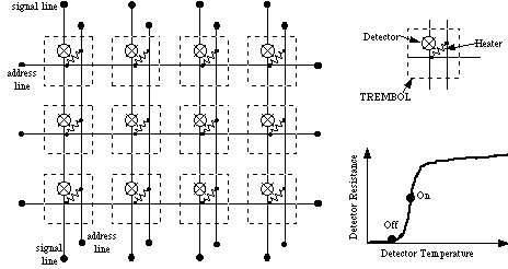
Fig. 5: Multiplexing in a composite TREMBOL array. A 3 x 4 array is shown
where each device consists of a heater connected to two address lines and
a detector connected to a signal line. The device is turned on by applying
enough heat to bring the detector to the center of the transition region.
5. DIRECTION OF FUTURE RESEARCH
The TREMBOL (transition-edge microbolometer) and the composite TREMBOL
have been introduced as detectors for FIR imaging arrays. The TREMBOL utilizes
a superconductor's sharp change in resistance at the normal conduction to
superconduction transition. The structure of the composite TREMBOL enables
heating of the individual detectors in an array up to their transition temperature,
and can thus be used in multiplexing, which would be very advantageous for
two-dimensional arrays.
Much work remains, however, to characterize the TREMBOL. A more thorough
study of the Pb device is needed, perhaps with the inclusion of a passivating
layer to protect the Pb from oxidizing. Other superconductors could be investigated
for this application, including the high Tc superconductors.
A composite TREMBOL mask set is presently being designed which will provide
for electroplated contacts on both the load/heater level and on the signal
line level. It will also contain a number of test structures, including
a signal line perpendicular to the bow-tie antenna.
6. ACKNOWLEDGEMENTS
The authors would like to thank Jason Lewis for his helpful suggestions.
This project was supported by the National Science Foundation under grant
#ECS-8552868.
7. REFERENCES
[1]. C.L. Bertin and K. Rose, "Radiant-Energy
Detection by Superconducting Films," J. Appl. Phys., Vol. 39,
No. 6, pp. 2561-2568, May 1968.
[2]. D.H. Andrews, R.M. Milton, and
W. DeSorbo, "A Fast Superconducting Bolometer," J. Opt. Soc.
Am., Vol. 36, No. 9, pp. 518-524, Sep. 1946.
[3]. D.H. Andrews, W.F. Brucksch,
Jr., W.T. Ziegler, and E.R. Blanchard, "Attenuated Superconductors:
I. For Measuring Infra-Red Radiation," Rev. Sci. Instrum., Vol.
13, pp. 281-292, July 1942.
[4]. J. Clarke, G.I. Hoffer, P.L.
Richards, and N.H. Yeh, "Superconductive bolometers for submillimeter
wavelengths," J. Appl. Phys., Vol. 48, No. 12, pp. 4865-4879,
Dec. 1977.
[5]. M. Scott, R.G. Keefe, and R.
Loehman, "High Transition Temperature Superconducting Infrared Detector,"
IEEE Trans. Electron Dev., Vol. 36, No. 1, pp. 62-65, Jan 1989.
[6]. K. Rose, "Superconductive
FIR Detectors," IEEE Transactions on Electron Devices, Vol.
ED-27, No. 1, pp. 118-125, Jan. 1980.
7 . J.M. Lewis, "Optical Detectors Based on Superconducting Bi-Sr-Ca-Cu-Oxide
Thin Films," B.S. Thesis, Mass. Inst. of Tech., June 1989.
8. P.L. Richards, F. Auracher, and T. Van Duzer, "Millimeter and Submillimeter
Wave Detection and Mixing with Superconducting Weak Links," Proc.
of the IEEE, pp. 36-45, Jan. 1973.
9. P.L. Richards, J. Clarke, R. Leoni, Ph. Lerch, S. Verghese, M.R. Beasley,
T.H. Geballe, R.H. Hammond, P. Rosenthal, and S.R. Spielman, "Feasibility
of the high Tc superconducting bolometer," Appl. Phys.
Lett., Vol. 54, No. 3, pp. 283-285, 16 Jan 1989.
[10]. D.P. Neikirk, "Integrated
detector arrays for high resolution far-infrared imaging," Ph.D. thesis,
California Inst. of Technol., pp. 148-149, 1984.
[11]. Q. Hu and P.L. Richards,"Design
analysis of a high Tc superconducting microbolometer," Appl.
Phys. Lett., Vol. 55, No. 23, pp. 2444-2446, 4 Dec. 1989.
[12]. S.M. Wentworth, R.L. Rogers,
J.G. Heston, D.P. Neikirk, and T. Itoh, "A MM Wave/FIR Twin Slot Antenna
on a Layered Substrate," to be published in Int. J. Infrared and
Millimeter Waves, Vol. 11, No. 2, Feb. 1990.
[13]. D.P. Neikirk, W.W. Lam, and
D.B. Rutledge, "Far-Infrared Microbolometer Detectors," Int.
J. Infrared and Millimeter Waves, Vol. 5, No. 3, pp. 245-278, Mar 1984.
[14]. S.M. Wentworth and D.P. Neikirk,
"Far-Infrared Composite Microbolometers," to be presented at the
1990 IEEE MTT-S International Microwave Symposium, Dallas, May 8-10,
1990.
[15]. J.G. Bednorz and K.A. Müller,
"Possible High Tc Superconductivity in the Ba-La-Cu-O System,"
Zeitschrift für Physik B, Vol. 64, pp. 189-193, 1986.
[16]. M.K. Wu, J.R. Ashburn, C.J.
Torng, P.H. Hor, R.L. Meng, L. Gao, A.J. Huang, Y.Q. Wang, and C.W. Chu,
"Superconductivity at 93 K in a New Mixed-phase Y-Ba-Cu-O Compound
System at Ambient Pressure," Phys. Rev. Lett., Vol. 58, No.
9, pp. 908-910, 2 Mar 1987.
[17]. H. Maeda, Y. Tanaka, M. Fukutomi,
and T. Asano, "A New High-Tc Oxide Superconductor without
Rare Earth Element," Jap. J. Appl. Phys., Vol. 27, p. L1209,
1988.
[18]. M.S. Osofsky, P. Lubitz, M.Z.
Harford, A.K. Singh, S.B. Qadri, E.F. Skelton, W.T. Elam, R.J. Soulen, Jr.,
W.L. Lechter, and S.A. Wolf, "Thin-film high Tc superconductors
prepared by a simple flash evaporation technique," Appl. Phys. Lett.,
Vol. 53, No. 17, pp. 1663-1664, 24 Oct. 1988.
19. M. Hong, S.H. Liou, J. Kwo, and B.A. Davidson, "Superconducting
Y-Ba-Cu-O oxide films by sputtering," Appl. Phys. Lett., Vol.
51, No. 9, pp. 694-696, 31 Aug 1987.
[20]. Z.L. Bao, F.R. Wang, Q.D.
Jiang, S.Z. Wang, Z.Y. Ye, K. Wu, C.Y. Li, and D.L. Yin, "YBaCuO superconducting
thin films with zero resistance at 84 K by multilayer deposition,"
Appl. Phys. Lett., Vol. 51, No. 12, pp. 946-947, 21 Sep 1987.
[21]. R.W. Simon, C.E. Platt, A.E.
Lee, G.S. Lee, K.P. Daly, M.S. Wire, J.A. Luine, and M. Urbanik, "Low-loss
substrate for epitaxial growth of high-temperature superconductor thin films,"
Appl. Phys, Lett., Vol. 53, No. 26, pp. 2677-2679, 26 Dec. 1988.
[22]. D.P. Neikirk, D.B. Rutledge,
and M.S. Muha, "Far-infrared imaging antenna arrays," Appl.
Phys. Lett., Vol. 40, No. 3, pp. 203-205, 1 Feb. 1982.
[23]. P.P. Tong, D.P. Neikirk, D.
Psaltis, D.B. Rutledge, K. Wagner, and P.E. Young, "Tracking Antenna
Arrays for Near-Millimeter Waves," IEEE Trans. Antennas Propagat.,
Vol. AP-31, No. 3, pp. 512-515, May 1983.