R. L. Rogers and D. P. Neikirk, "Use of Broadside Twin Element Antennas to Increase Efficiency on Electrically Thick Dielectric Substrates," Int. J. Infrared Millimeter Waves, vol. 9, pp. 949-969, 1988.
R. L. Rogers, "A Study of Slot and Dipole Antennas on Layered Electrically Thick Dielectric Substrates for Far Infrared and Millimeter Wave Imaging Arrays," 1989, PhD, The University of Texas at Austin.
R. L. Rogers and D. P. Neikirk, "Radiation Properties of Slot and Dipole Elements on Layered Substrates," Int. J. Infrared Millimeter Waves, vol. 10, pp. 697-728, 1989.
S. M. Wentworth, R. L. Rogers, J. G. Heston, D. P. Neikirk, and T. Itoh, "Millimeter Wave Twin Slot Antennas on Layered Substrates," Int. J. Infrared Millimeter Waves, vol. 11, pp. 111-131, 1990.
S.M.Wentworth, R.L. Rogers, J.G. Heston, and D.P. Neikirk, "Twin-slot multi-layer substrate-supported antennas and detectors for terahertz imaging," First International Symposium on Space Terahertz Technology, University of Michigan, Ann Arbor, Mich., March 5-6, 1990, pp. 201-213.
J.G. Heston, S.M. Wentworth, R.L. Rogers, D.P. Neikirk, and T. Itoh, "MM Wave /FIR Twin Slot Antenna Structures," AP-S International Symposium and URSI Radio Science Meeting, May, 1990.
J.G. Heston, J.M. Lewis, S.M. Wentworth, and D.P. Neikirk, "Twin slot antenna structures integrated with microbolometer detectors for 94 GHz imaging," Microwave and Optical Technology Letters 4, no. 1, Jan. 5, 1991, pp. 15-19.
Twin-slot Multi-layer Substrate-supported Antennas
and Detectors for Terahertz Imaging*
Stuart M. Wentworth, Robert L. Rogers, John G. Heston, and Dean P. Neikirk
The University of Texas at Austin
Austin, TX 78712
*Please see the complete paper: S.M.Wentworth, R.L. Rogers, J.G. Heston, and D.P. Neikirk, "Twin-slot multi-layer substrate-supported antennas and detectors for terahertz imaging," First International Symposium on Space Terahertz Technology, University of Michigan, Ann Arbor, Mich., March 5-6, 1990, pp. 201-213.
Planar antenna arrays with integrated detectors have proven to be very
useful for millimeter and submillimeter wave receiver systems. One problem
with planar antennas is their tendency to couple significant power into
guided modes (also called surface waves) when the substrate is a significant
fraction of a dielectric wavelength ![]() thick [1].
Coupling into these surface waves can be avoided by making the substrate
very thin (on the order of 50 micron or less for far-infrared radiation),
or by making the substrate appear infinitely thick by placing a focusing
lens on back of the substrate [2]. Unfortunately, substrate
lenses tend to be quite lossy in the terahertz regime, while membrane-supported
devices present difficult fabrication challenges. A third approach involves
the use of electrically thick substrates of carefully chosen thickness,
in conjunction with an antenna design which suppresses surface wave coupling.
thick [1].
Coupling into these surface waves can be avoided by making the substrate
very thin (on the order of 50 micron or less for far-infrared radiation),
or by making the substrate appear infinitely thick by placing a focusing
lens on back of the substrate [2]. Unfortunately, substrate
lenses tend to be quite lossy in the terahertz regime, while membrane-supported
devices present difficult fabrication challenges. A third approach involves
the use of electrically thick substrates of carefully chosen thickness,
in conjunction with an antenna design which suppresses surface wave coupling.
In this paper we will discuss twin-slot antennas supported on a multilayer dielectric stack, which show both good patterns and efficiencies. The dielectric layers used are thick enough to be handled with conventional fabrication equipment. The appropriate choice of dielectric stack also allows the beamwidth to be adjusted, providing a good match between the antenna and optical system feed patterns. In addition, we will also discuss new integrated microbolometer configurations which should be more sensitive than conventional microbolometers for terahertz detection. The combination of these antennas and detectors may allow the fabrication of imaging arrays with higher sensitivities than those currently available.
The theory underlying a twin slot antenna on a dielectric stack (Fig. 1) has been covered in extensive detail by Rogers et al. [3-5]. In this theory, it is much easier to treat the twin slot antenna structure as a source of radiation rather than as a receiver. By reciprocity, efficiencies and beam patterns will be the same for both source and receiver. Briefly, the total power emitted by a twin slot antenna consists of the power radiated through the dielectric (the "front side" of the structure), the power lost to surface waves, and the power radiated directly to air (the "backside" of the structure). To calculate radiated power, equivalent transmission line models of the dielectric stack are used, and each slot is modeled as a voltage source. To calculate power lost to surface waves, a reciprocity method described by Rutledge et al. is used [6].
Planar antennas placed on a dielectric substrate tend to radiate more
power through the dielectric than directly into air [6].
For most efficient operation, it is desirable that the power radiated through
the dielectric side be much larger than that radiated directly to air (i.e.,
to the backside of the stack). For a slot antenna, the use of an odd number
of ![]() thick dielectric layers, with high-low-high alternating
dielectric constants, will maximize the frontside radiation [3,8]. The dielectric substrate which supports the antenna
also forms a waveguide structure which will cause undesirable loss of power
to guided (or surface) waves. However, if the substrate consists of an odd
number of
thick dielectric layers, with high-low-high alternating
dielectric constants, will maximize the frontside radiation [3,8]. The dielectric substrate which supports the antenna
also forms a waveguide structure which will cause undesirable loss of power
to guided (or surface) waves. However, if the substrate consists of an odd
number of ![]() thick layers, alternating from high to low to high dielectric
constant, it is possible to restrict the surface wave losses to one dominant
mode, usually the TMo mode [9]. If a pair of slots is
placed one half a TMo wavelength apart in the broadside direction, and the
slots are driven in-phase, then the TMo modes from each slot will superimpose
and cancel [4]. Thus, the same dielectric stack which
maximizes radiated power through the dielectric can also be used to suppress
surface wave losses when used in conjunction with twin slots. Similar twin
slot antennas have been used in the past as a component in a quasi-optical
mixer operating at 100 to 120 GHz [10].
thick layers, alternating from high to low to high dielectric
constant, it is possible to restrict the surface wave losses to one dominant
mode, usually the TMo mode [9]. If a pair of slots is
placed one half a TMo wavelength apart in the broadside direction, and the
slots are driven in-phase, then the TMo modes from each slot will superimpose
and cancel [4]. Thus, the same dielectric stack which
maximizes radiated power through the dielectric can also be used to suppress
surface wave losses when used in conjunction with twin slots. Similar twin
slot antennas have been used in the past as a component in a quasi-optical
mixer operating at 100 to 120 GHz [10].
In order to test the performance of the dielectric stack structures twin slot antennas have been fabricated on a 2.5 cm x 2.5 cm square 406 micron thick fused quartz substrates for operation near 94 GHz [11]. The slot ground plane was deposited by thermal evaporation of ~30 nm of chromium for adhesion followed by ~600 nm of gold (slightly more than two skin depths at 94 GHz). Slots were then chemically etched into the ground plane. The feed network was separated from the ground plane by a 2 micron thick polyimide layer (DuPont Pyralin PI-2556 polyimide), cured at 250 deg.C for a duration of 1.5 hours. Fabrication of bismuth microbolometer detectors and microstrip feed line network was accomplished using a bilayer photoresist bridge technique [12,13]. The Bi microbolometer was approximately 100 nm thick, 3 micron long and 3 micron wide. The feed lines are 25 micron wide,with a 100 nm thick layer of Ag topped by a 200 nm thick layer of Bi, and finally a 200 nm thick layer of Ag (the much higher conductivity of Ag essentially shorts the Bi in the feed line). Bi microbolometer resistance was measured to be about 80 ohm, and the microstrip impedance was calculated to be about 13-16 ohm based on empirical formulas [14, 15, 16]. The series resistance of the microstrip line between the innermost filters was measured as 18 ohm (~0.23 ohm/square). For the fused quartz structure, the room temperature microbolometer responsivity was measured to be about 7.2 V/W when biased at 0.1 V.
Electrical connection was achieved by placing the chip on a small microwave laminate board, and connecting pads on the chip to copper pads on the board using silver paint. The chip was placed in a positioning mount with the twin slot antenna at the center, allowing the antenna to pivot in the E- and H-planes. A Hughes IMPATT W-band oscillator connected to a standard gain horn was placed approximately 36 cm from the antenna. Laser alignment was used to determine boresight and to align the chip plane parallel with the plane of the horn. The radiation was chopped at 200 Hz, and the signal was measured with a Stanford Research Systems SR530 lock-in amplifier. Measurements were taken at 4deg. increments in both E- and H-planes, and the detected signals ranged from 6 microV down to the background noise level of about 0.02 microV.
Figure 2 shows both measured and calculated receiver gain beam patterns for the single fused quartz substrate operating at 90.5 GHz. There is considerable asymmetry between the E- and H-planes, which would be undesirable for optical system feeds. The shape of the measured E-plane agrees reasonably well with the theoretical model. We conjecture that the slightly jagged peaks are associated with finite ground plane effects, and with interference from surface waves reflecting back from the edges of the ground plane. The shape of the H-plane beam pattern shows only rough agreement with theory. We again assume that this is primarily a result of guided waves reflecting off the ground plane edge. There may also have been interference from adjacent pairs of slots, which were 0.5 cm distant from the center element in the H-plane. The sudden drop for the H-plane pattern at -56deg. is due to shadowing from the antenna positioner mount.
Placement of a quarter wavelength thick quartz layer one quarter of a
wavelength above the substrate tested above results in a "resonant"
structure similar to those described in [8]. The quartz-air-quartz
stack, corresponding to ![]() = 3.8 and
= 3.8 and ![]() = 1.0 in Fig.
1, was made by placing a 1/4
= 1.0 in Fig.
1, was made by placing a 1/4 ![]() thick (406 micron) fused
quartz chip over the substrate, using small spacers 860 micron thick
placed at the corners of the chip. Figures 3 and 4 show beam patterns for
this multilayer stack at 90.5 and 94 GHz, respectively. Although the antenna
is designed for 94 GHz, the air gap was slightly thicker (~864 micron) than
the 1/4
thick (406 micron) fused
quartz chip over the substrate, using small spacers 860 micron thick
placed at the corners of the chip. Figures 3 and 4 show beam patterns for
this multilayer stack at 90.5 and 94 GHz, respectively. Although the antenna
is designed for 94 GHz, the air gap was slightly thicker (~864 micron) than
the 1/4 ![]() design thickness (787 micron). Experimentally, the narrowest
beam pattern was found at 90.5 GHz, which matched the predicted resonant
frequency for the actual layer thicknesses used. In both figures, the calculated
beam pattern shapes are approximately matched by experiment. The boresight
gain does not change noticeably between 94 and 90.5 GHz. This could be quite
convenient in lens-coupled receivers where the beam pattern is not critical,
but where the gain is desired constant over some appreciable bandwidth.
design thickness (787 micron). Experimentally, the narrowest
beam pattern was found at 90.5 GHz, which matched the predicted resonant
frequency for the actual layer thicknesses used. In both figures, the calculated
beam pattern shapes are approximately matched by experiment. The boresight
gain does not change noticeably between 94 and 90.5 GHz. This could be quite
convenient in lens-coupled receivers where the beam pattern is not critical,
but where the gain is desired constant over some appreciable bandwidth.
Comparing the single and multilayer 90.5 GHz results of Figs. 2 and 3, the theory predicts a boresight gain about 6 dB higher for the multilayer case. This increase is indeed observed since the boresight detector signal increases from 1 microV to 4 microV when the additional layer and air gap are added. It is also observed that compared to the single layer case, the measured and calculated patterns for the multilayer case are much narrower, and would thus match an optical system of higher f-number.
Our model predicts at least a 10 dB higher receiver gain than is achieved by any of the experimental cases. However, the theory does not consider losses in the feedline, nor does it consider mismatch losses between the detector and the feed line. Our measurements indicate 6 dB of feedline loss. Another 3 dB mismatch loss is expected between the detector (80 ohm resistance) and the microstrip feedline (13-16 ohm impedance). Another possible loss mechanism is rf power loss through the low pass filters, which may not have a low enough impedance compared to the microstrip line.
The twin slot antennas discussed above made use of integrated microbolometer detectors. These detectors are relatively simple to fabricate, present a purely real impedance, and can easily be calibrated to make absolute power measurements. Figure 5 shows the dependence of resistance on ambient temperature for microbolometers made of bismuth and of tellurium [17]. These devices were about 100 nm thick and roughly 4 micron x 4 micron in area, and were fabricated on glass substrates. The slopes for both materials stay fairly constant throughout the temperature range measured. The dR/dT of Te is roughly 3 orders of magnitude higher than that of Bi. Calculations show that a microbolometer made with Te could approach responsivities of magnitude 2000 V/W, or a hundred times higher than a comparable Bi microbolometer. Although the Te looks promising because of its high responsivity, its high resistance makes direct coupling to a planar antenna difficult. However, alternative composite structures for impedance matching could be developed to utilize such high resistance detectors. The combination of new antenna structures and high responsivity microbolometers may allow a significant improvement in far-infrared detector sensitivity.
One solution to the mismatched load problem is to separate the load from the detector in a composite microbolometer structure, as shown in Fig. 6 [18]. The load, which is impedance-matched to the antenna, is in intimate thermal contact with, but is electrically isolated from, the detector element. Changes in load temperature will be quickly followed by changes in detector temperature, and hence by changes in detector resistance.
Composite microbolometers have been fabricated on glass substrates consisting of nichrome as the load, Te as the detector, and SiO]x as the insulator. The 80% Ni-20% Cr load was approximately 150 nm thick, in contact with a 150 nm thick gold bow-tie antenna. Following deposition of an 180 nm thick SiOx layer, the signal line/detector layer was fabricated. The Te detector was about 120 nm thick, contacted to a 200 nm thick gold signal line. The lengths and widths were about the same for both NiCr and Te elements, ranging from 4.5 to 5.0 micron. Fabrication will be detailed elsewhere [18].
Figure 7 shows the responsivity curve generated for the composite microbolometer
at a Te detector bias of 0.75 V. This figure also shows the noise voltage
measured across the Te detector element at the same voltage. The noise is
measured with a PAR 124A lock-in amplifier with 117 preamp over a bandwidth
of 10% of the selected center frequency. Since the Johnson noise floor is
about 10**-8 ![]() , it is clear from this figure that a 1/f-type noise
is dominant. The NEP plot in Fig. 8 is calculated by dividing the noise
by the responsivity. The device has a minimum NEP of 6.7 x 10**-9
, it is clear from this figure that a 1/f-type noise
is dominant. The NEP plot in Fig. 8 is calculated by dividing the noise
by the responsivity. The device has a minimum NEP of 6.7 x 10**-9
![]() at 30 kHz. For comparison, a Bi microbolometer typically
has an rdc of 20 V/W, and minimum NEP of 10**- 10
at 30 kHz. For comparison, a Bi microbolometer typically
has an rdc of 20 V/W, and minimum NEP of 10**- 10 ![]() at 10 kHz. Although
the NEP of our composite microbolometer is somewhat higher than a conventional
Bi device, the higher responsivity produces signals of much larger magnitude,
thus reducing the requirements for very small signal amplifiers. Also, it
is somewhat easier to build low noise amplifiers which match the higher
input impedance of the composite detectors.
at 10 kHz. Although
the NEP of our composite microbolometer is somewhat higher than a conventional
Bi device, the higher responsivity produces signals of much larger magnitude,
thus reducing the requirements for very small signal amplifiers. Also, it
is somewhat easier to build low noise amplifiers which match the higher
input impedance of the composite detectors.
A planar receiver has been demonstrated which consists of a twin slot antenna on a dielectric stack and a microbolometer detector. As expected from theory, a higher gain beam pattern was obtained when a quartz-air-quartz dielectric stack was used. Both theoretical models and experimental measurements show that although all the dimensions used for this antenna structure (i.e. the dielectric layer thicknesses, slot length, slot separation, and microstrip feed network length) are referenced to a single design frequency, the operating bandwidth is reasonably broad, without dramatic changes in either gain or pattern over at least a 5% variation in frequency.
A composite microbolometer has also been developed using a NiCr load and a Te detector element. Such a structure removes the constraint of impedance matching to the antenna impedance, and opens the way for the use of a variety of new materials with considerably larger temperature coefficients of resistance than bismuth.
1. 1. B. Roudot, J. Mosig, and F. Gardiol, "Surface Wave Effects on Microstrip Antenna Radiation," Microwave Journal, pp. 201-211, March 1988.
2. D.P. Neikirk, D.B. Rutledge, M.S. Muha, H. Park, and C.X. Yu, "Progress in millimeter-wave integrated circuit imaging arrays," Proc. SPIE, 317, p. 206, 1981. 3. R.L. Rogers and D.P. Neikirk, "Radiation Properties of Slot and Dipole Elements on Layered Substrates," Int. J. Infrared and Millimeter Waves, Vol 10, No. 6, pp. 697-728, 1989.
4. R.L. Rogers and D.P. Neikirk, "Use of Broadside Twin Element Antennas to Increase Efficiency on Electrically Thick Dielectric Substrates," Int. J. Infrared and Millimeter Waves, Vol. 9, No. 11, pp. 949-969, 1988.
5. R.L Rogers, S.M. Wentworth, D.P. Neikirk, and T. Itoh, "A twin slot antenna on a layered substrate coupled to a microstrip feed line," Int. J. Infrared and Millimeter Waves 11, no. 10, October 1990, pp. 1225-1249.
6. D.B. Rutledge, D.P. Neikirk, and D.P. Kasilingam, "Integrated Circuit Antennas," Infrared and Millimeter Waves, Vol. 10, Academic Press, pp. 1-90, 1983.
7. N.G. Alexopoulos, P.B. Katehi, and D.B. Rutledge, "Substrate Optimization for Integrated Circuit Antennas," IEEE Trans. MTT, Vol. 31, No. 7, pp. 550-557, 1983.
8. N.G. Alexopoulos and D.R. Jackson, "Fundamental Superstrate Effects on Printed Circuit Antennas," IEEE Trans. Antennas and Propagation, Vol. AP-32, No. 8, pp. 807-816, Aug. 1984.
9. R.L. Rogers, D.P. Neikirk, H. Ling, and T. Itoh, "Antennas on Layered Substrates," 13th Annual Conf. on Infrared and Millimeter Waves, pp. 33-34, Dec. 1988.
10. A.R. Kerr, P.H. Siegel, and R.J. Mattauch, "A simple quasi-optical mixer for 100-120 GHz," in 1977 IEEE MTT-S Int. Microwave Symposium Dig., pp. 96-98.
11. S.M. Wentworth, R.L. Rogers, J.G. Heston, D.P. Neikirk, and T. Itoh, "Millimeter Wave Twin Slot Antennas on Layered Substrates," Int. J. Infrared and Millimeter Waves, Vol. 11, No. 2, Feb. 1990, pp. 111-131.
12. D.P. Neikirk, W.W. Lam, and D.B. Rutledge, "Far-Infrared Microbolometer Detectors," Int. J. Infrared and Millimeter Waves, Vol. 5, No. 3, pp. 245-278, 1984.
13. D. M. Dobkin and B. D. Cantos, "Plasma Formation of Buffer Layers for Multilayer Resist Structures," IEEE Electron Device Lett., Vol. EDL-2, No. 9, pp. 222-224, Sept. 1981.
14. T.C. Edwards, Foundations for Microstrip Circuit Design, Wiley and Sons, New York, 1981, pp. 44-47.
15. K.C. Gupta, R. Garg, I.J. Bahl, Microstrip Lines and Slotlines, Artech House, Inc. 1979, p. 11.
16. I. Bahl and P. Bhartia, Microwave Solid State Circuit Design, Wiley and Sons, New York, 1988, p. 18.
17. S.M. Wentworth and D.P. Neikirk, "Far Infrared Microbolometers Made with Tellurium and Bismuth," Electronics Letters[,Vol. 25, No. 23, pp. 1558-1560, 9 Nov. 1989.
18. S.M. Wentworth and D.P. Neikirk, "Far-Infrared Composite Microbolometers," IEEE MTT-S International Microwave Symposium Digest, Vol. III, May 8-10, 1990, pp. 1309-1310.
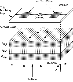
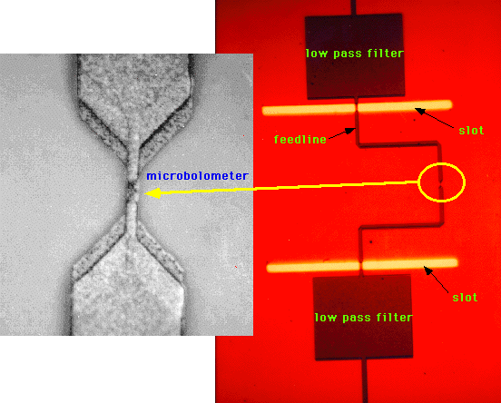
Fig. 1: Twin slot antenna on a dielectric stack, where each layer is 1/4 wavelength thick. The slots couple power into a microstrip line supported over the slots by a thin insulator. This power is dissipated in a detector, and is isolated from the rest of the feed network by low pass filters.
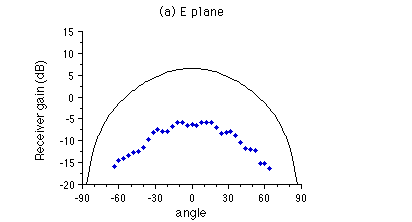
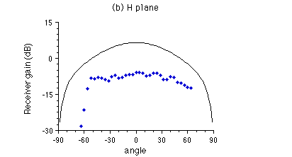
Fig. 2: (a) E-plane and (b) H-plane beam patterns for a twin slot antenna
on a single 1/4 ![]() thick fused quartz substrate for 90.5
GHz radiation. Theory (solid line) is compared with experiment.
thick fused quartz substrate for 90.5
GHz radiation. Theory (solid line) is compared with experiment.
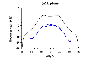
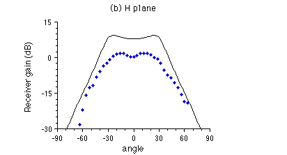
Fig. 3: (a) E-plane and (b) H-plane beam patterns for a twin slot antenna on a multilayer stack (dielectric constants 3.8,1, and 3.8) for 94 GHz radiation. Theory (solid line) is compared with experiment.
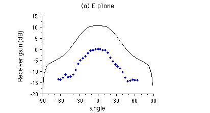
Fig. 4: (a) E-plane and (b) H-plane beam patterns for a twin slot antenna on a multilayer stack (dielectric constants 3.8,1, and 3.8) for 90.5 GHz radiation. Theory (solid line) is compared with experiment.
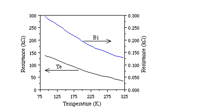
Fig 5: Resistance as a function of temperature for Te and Bi microbolometers.
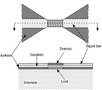
Fig. 6: Top view and cross section of a composite microbolometer. The load is impedance-matched to the bow-tie antenna, and is thermally coupled to a detector.
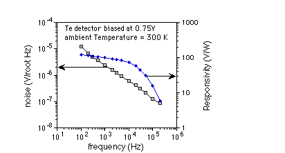
Fig. 7 Noise and responsivity are plotted versus beat frequency for a composite microbolometer with the Te detector element biased at 0.75V.
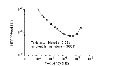
Fig. 8: Sensitivity for the composite microbolometer versus beat frequency,
with the Te detector element biased at 0.75V. Best performance occurs at
about 30 kHz, where NEP = 6.7 x 10**-9 ![]() .
.