AlAs/In0.53Ga0.47As Depletion Edge Modulated QWITT (DEMQWITT) Diode
Vijay Reddy, Shiva Javalagi, and Dean P. Neikirk
Microelectronics Research Center and the Department of Electrical and Computer Engineering
The University of Texas at Austin
Austin, TX 78712
Also see summaries of our work on:
The optimum length of the depletion region in a QWITT diode (Wopt) can
be quite long; for example, low injection conductance ([[sigma]]) devices
QWITTs have been grown that would require a Wopt of approximately 1.2 micron.
Fabricating a QWITT structure with such a large W would be impractical for
two reasons. First, given the magnitudes of the electric fields involved,
it would be extremely difficult to completely deplete one micron. Second,
the peak voltage would be extremely high and result in low DC-to-RF conversion
efficiency oscillators. For oscillator applications, increasing the ![]() product (the product of the difference between the peak and valley voltages
and the difference between the peak and valley currents) to improve the
RF output power is the prime concern. However, it is also desirable to decrease
Vp as this will reduce the required bias voltage and result in improved
DC-to-RF conversion efficiency. This can be done by inserting a doping spike
(a heavily doped layer) between the quantum well and the drift region. A
properly designed doping spike will reduce the electric field in the drift
region but yet fully deplete the drift region. The end result is a reduction
in Vp with
product (the product of the difference between the peak and valley voltages
and the difference between the peak and valley currents) to improve the
RF output power is the prime concern. However, it is also desirable to decrease
Vp as this will reduce the required bias voltage and result in improved
DC-to-RF conversion efficiency. This can be done by inserting a doping spike
(a heavily doped layer) between the quantum well and the drift region. A
properly designed doping spike will reduce the electric field in the drift
region but yet fully deplete the drift region. The end result is a reduction
in Vp with ![]() remaining unchanged. Kesan et al. have employed this
technique to reduce Vp and increase the conversion efficiency in AlAs/GaAs
QWITTs [1].
remaining unchanged. Kesan et al. have employed this
technique to reduce Vp and increase the conversion efficiency in AlAs/GaAs
QWITTs [1].
Another approach can be taken to achieve the same goal of reducing Vp
without sacrificing ![]() . Although this technique employs a doping spike, it
is fundamentally different from the doping spike method. Recall that the
quantum well injector characteristic can be extracted from the J - V curve
by accounting for voltage drops due to series parasitic series resistance
and space charge regions surrounding the double barrier structure. The injector
characteristic for the AlAs/In0.53Ga0.47As quantum well used in this study
is shown in Fig. 4.12.
. Although this technique employs a doping spike, it
is fundamentally different from the doping spike method. Recall that the
quantum well injector characteristic can be extracted from the J - V curve
by accounting for voltage drops due to series parasitic series resistance
and space charge regions surrounding the double barrier structure. The injector
characteristic for the AlAs/In0.53Ga0.47As quantum well used in this study
is shown in Fig. 4.12.
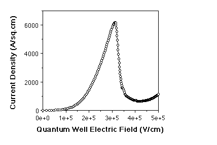
Fig. 4.12 Quantum well injector characteristic of AlAs/In0.53Ga0.47As quantum well used in DEMQWITT study. Provided by K. Gullapalli.
From Eq. 4.12, Wopt is inversely proportional to the differential conductance of the injector characteristic. From Fig. 4.12 it is clear that near the peak, Wopt is small because of the high differential conductance. However, in much of the NDR region, the optimum length is very large because of the very low differential conductance. Therefore, by grading the doping profile in the drift region from high to low, it should be possible to obtain depletion region lengths that are optimum at each point in the NDR region of the injector characteristic. Note that such a design, where the depletion edge is modulated during the rf cycle, is very different from the conventional QWITT design where the depletion region length is fixed. Therefore, this device has been named the depletion edge modulated QWITT or DEMQWITT.
A DEMQWITT with the layer schematic shown in Fig. 4.13 was fabricated. The downstream layer doping profile consists of a 215 Å, three step dopant transition layer adjacent to the AlAs barrier, a 210 Å heavily doped spike layer, and finally a 1 um thick, nominally undoped drift region. The background carrier concentration in the drift region is assumed to be n-type, 1 x 1016 cm-3. The measured I - V characteristic in reverse bias (DEMQWITT mode) is shown in Fig. 4.14.
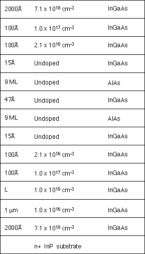
Fig. 4.13 Layer schematic of AlAs/In0.53Ga0.47As DEMQWITT. The doping spike thickness, L, is 210 Å. The 1 micron layer is nominally undoped and assumed to be n-type, 1 x 1016 cm-3.
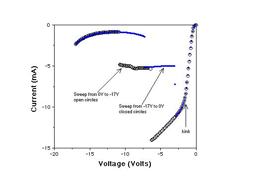
Fig. 4.14 Measured I - V characteristic of L = 210 Å AlAs/In0.53Ga0.47As DEMQWITT. The voltage is swept from 0 V to -17V (open circles) and back to 0 V (closed circles). The hysteresis is due to the difference in the start-up condition for oscillation and the space-charge resistance due to the 1 micron lightly doped drift region.
A few remarks should be made about the I - V curve. What is quite remarkable is the extended valley region, approximately ten volts. This is much larger than the two volts achieved with the low [[sigma]] QWITTs discussed in the previous section. In the PDR region before the peak, the kink that appears as the PDR slope changes is due to the electric field being insufficiently screened by the doping spike layer. The region of the I - V curve between the kink point and the peak represents the electric field punch through into the lightly doped region. Apparent in the figure is the hysteresis as the voltage is swept from 0 V to -17 V and back to 0 V. This is due to the difference in the start-up condition for oscillation and the space-charge resistance due to the 1 micron lightly doped drift region. To improve the characteristics, the doping spike layer should either be thicker or have a higher doping concentration. Furthermore, the 1 um drift region doping was probably lower than the assumed value of 1 x 1016 cm-3.
Despite the spectacular ![]() available with the DEMQWITT, application
to microwave oscillators is limited to low frequency (few GHz) operation
by the device's low Jp. To avoid large peak voltages and possible catastrophic
breakdown, DEMQWITTs can only be fabricated if the Jp is low enough that
the electron concentration required to support Jp is less than the background
doping concentration. Furthermore, the requirement that 1 micron be totally
depleted places an upper limit on the background doping concentration, thus
again limiting Jp. Nevertheless, the DEMQWITT is a promising device at low
gigahertz frequencies for applications requiring high power, high efficiency
operation.
available with the DEMQWITT, application
to microwave oscillators is limited to low frequency (few GHz) operation
by the device's low Jp. To avoid large peak voltages and possible catastrophic
breakdown, DEMQWITTs can only be fabricated if the Jp is low enough that
the electron concentration required to support Jp is less than the background
doping concentration. Furthermore, the requirement that 1 micron be totally
depleted places an upper limit on the background doping concentration, thus
again limiting Jp. Nevertheless, the DEMQWITT is a promising device at low
gigahertz frequencies for applications requiring high power, high efficiency
operation.