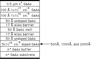
Fig. 1: A schematic cross section of the QWITT structures examined in this study.
also see:
V.P. Kesan, A. Mortazawi, D.R. Miller, T.Itoh, B.G. Streetman, and D.P.
Neikirk, "Microwave Frequency Operation of the Quantum Well Injection
Transit Time (QWITT) Diode," Electronics Letters 24, 24 Nov.
1988, pp. 1473-1474.
V.P. Kesan, A. Mortazawi, D.R. Miller, V.K. Reddy, D.P. Neikirk, and T.
Itoh, "Microwave and Millimeter Wave QWITT Diode Oscillators,"
IEEE Trans. Microwave Theory Tech. MTT-37, Dec. 1989, pp. 1933-1941.
S. Javalagi, V. Reddy, K. Gullapalli, and D. Neikirk, "High
efficiency microwave diode oscillators," Electronics Letters
28, 27 August 1992, pp. 1699-1701.
also see our work on the theoretical behavior of double barrier resonant tunneling diodes with spacer layers:
Influence
of Space Charge and Quantum Well Negative Resistances on Resonant Tunneling
Diodes
V. P. Kesan, A. Mortazawi, D. R. Miller, V. K. Reddy, A.
Tsao, and D.P. Neikirk
Department of Electrical and Computer Engineering
The University of Texas at Austin, Austin, Texas 78712
DC and microwave characteristics of different QWITT structures are discussed. A peak output power of ~ 1 mW in the frequency range of 2-10 GHz has been obtained. At the time of publication of the original work (Nov. 1988) this was the highest output power obtained from any quantum well oscillator at any frequency. We will show that, for the same quantum well structure, by systematically increasing the length of the depletion region (i.e., the drift region) on the anode side of the device a corresponding increase in the specific negative resistance and output power is obtained. The significant increase in output power clearly suggests that the intrinsic device characteristics have been improved through the use of a drift region. This is in keeping with small-signal analysis for the QWITT diode, which predicts an improvement in the rf performance of the device with the use of an appropriate drift region length for a particular frequency of operation.
Quantum well oscillators have been shown to be capable of generating
power at high millimeter wave frequencies [1, 2], and there has been expectation
that these devices could serve as a useful local oscillator at frequencies
between 100-1000 GHz. However, there has been considerable debate over the
quantum well device structures that must be used to maximize the output
power obtained from these devices.
We have proposed an improved quantum well oscillator, the quantum well injection
transit time (QWITT) diode [3], consisting of a double barrier structure
coupled with a depletion region which increases the specific negative resistance
and impedance of the device so that higher output power can be obtained.
We have performed both small- and large-signal analyses [4-6] of the QWITT
diode in order to develop a model that relates physical device and material
parameters to the output performance of the device. A large-signal model
for the QWITT diode has also been presented by Song and Pan [7].
A schematic diagram of one set of device structures used in our studies
are shown in Fig. 1. Three structures, A, B, and C, consisting of identical
quantum well regions but with three different drift region lengths of 500
Å, 1000 Å, and 2000 Å respectively, were examined. The
heterolayers were grown in a Varian GEN II MBE system on n+,
(100) GaAs substrates (Airtron-Litton), silicon doped to 3x10¹⁸
cm-3. Device mesas were defined using conventional photolithographic
techniques and etched using 4:1:1 H2SO4:H2O2:H2O. Devices had a nominal
area of 3.3-3.8x10⁻⁷ cm2 with a height of around 0.5
um. Top ohmic contacts were formed using AuGe/Ni and alloying at 450deg.
C for 30 secs. Pulsed (50% duty cycle) and continuous dc current-voltage
characteristics at 300 K were measured.
Fig. 1: A schematic cross section of the QWITT structures examined in this
study.
The dc characteristics for the three devices shown in Figure 1 are summarized
in Table I. As expected, due to the asymmetric structure of the QWITT diode,
the dc I-V characteristics for the two bias directions are very different.
In any negative resistance diode the voltage and current differences between
peak and valley, ![]() and
and ![]() , must be as large as possible to increase
the device output power; in a low frequency model power is directly proportional
to
, must be as large as possible to increase
the device output power; in a low frequency model power is directly proportional
to ![]() . For the QWITT diode,
. For the QWITT diode, ![]() is increased through
the use of a drift region, but
is increased through
the use of a drift region, but ![]() should remain virtually the same
as the intrinsic quantum well. This results in an increase in the total
output power that can be obtained from the QWITT diode compared to a bare
resonant tunneling diode. We can see that while the variation in peak-to-valley
current differences,
should remain virtually the same
as the intrinsic quantum well. This results in an increase in the total
output power that can be obtained from the QWITT diode compared to a bare
resonant tunneling diode. We can see that while the variation in peak-to-valley
current differences, ![]() , for the three devices A, B, and C,
is quite small, a large increase in
, for the three devices A, B, and C,
is quite small, a large increase in ![]() is observed in these devices
(Table I). For the QWITT bias mode (forward bias, substrate positive), as
the length of the drift region is increased from 500Å to 2000Å,
the voltage corresponding to the current peak, Vp, increases from 2.4V to
5.5V, and the voltage difference between peak and valley currents,
is observed in these devices
(Table I). For the QWITT bias mode (forward bias, substrate positive), as
the length of the drift region is increased from 500Å to 2000Å,
the voltage corresponding to the current peak, Vp, increases from 2.4V to
5.5V, and the voltage difference between peak and valley currents, ![]() ,
also increases from 0.3V to 1.18V. For each device structure, when electrons
are injected from the substrate to the top (reverse bias, substrate negative)
,
also increases from 0.3V to 1.18V. For each device structure, when electrons
are injected from the substrate to the top (reverse bias, substrate negative)
![]() is smaller as compared to when electrons are injected from
the top to the substrate (forward bias). This is because in reverse bias
the n- GaAs drift region is under accumulation, and can add only
positive series resistance to the device, thus reducing
is smaller as compared to when electrons are injected from
the top to the substrate (forward bias). This is because in reverse bias
the n- GaAs drift region is under accumulation, and can add only
positive series resistance to the device, thus reducing ![]() , as opposed to
the QWITT mode, where this region actually contributes to the negative resistance
of the device.
, as opposed to
the QWITT mode, where this region actually contributes to the negative resistance
of the device.
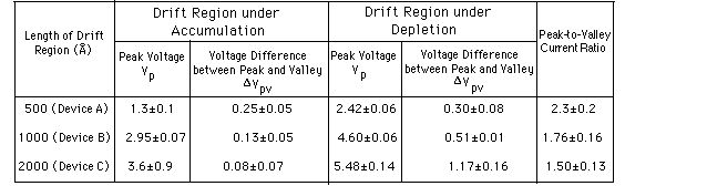
Table I: DC characteristics in both bias directions for the devices studied.
To determine the microwave characteristics of the devices shown in Fig.
1 they were mounted in a WR-90 (8.2-12.4 GHz) waveguide (Fig. 2) using a
micrometer-controlled post and whisker-contacted for microwave measurements.
In addition, the devices were mounted in a planar oscillator circuit consisting
of a microstrip line with a dielectric resonator (Fig. 3). The rf measurements
were made using a Tektronix 492AP spectrum analyzer and the output power
measurements were verified using an Anritsu rf power meter.
The microwave performance of the three QWITT structures is summarized in
Table II. Two rf circuits have been tested: a whisker-contacted post mount
in a WR-90 waveguide backed by a sliding short, and a planar circuit consisting
of a microstrip line with a dielectric resonator, using a long wire whisker
to make contact between microstrip and the QWITT diode. A coaxial triple
stub tuner was also used to improve matching between the diode circuits
and 50 Ohm characteristic impedance measurement instruments. The oscillation
frequency in the waveguide circuit could be varied from 8 to 12 GHz by changing
the dc bias and the position of the sliding short. With the microstrip circuit
oscillations in the frequency range of 2-8 GHz were detected, with a peak
output power of ~ 1 mW from device C. The impedance of the planar oscillator
circuit is much lower than the waveguide circuit, and the improvement in
output power seen in the planar circuit is probably due to a better match
to the low impedance of the device. For the different devices, as the length
of the drift region is increased from 500 Å to 2000 Å, the output
power increases dramatically in both oscillator circuits (Table II). No
attempt was made to optimize the microwave resonant cavity and improve the
output power by using either reduced height waveguide or improving the circuit
impedance match in the planar circuit. In addition, the device areas used
in this study were not optimized [5], and intentionally kept small to avoid
excessive heating and consequent heat sinking problems. However, the dramatic
increase in output power obtained in devices B and C compared to device
A clearly suggests that, as predicted by previous analyses [4-6], the intrinsic
device characteristics have been improved through an appropriate choice
of drift region length.
Length of drift region (Å) |
DC negative resistance (ohms) |
Output power (microWatts) |
Oscillation frequency (GHz) |
500 (Device A) |
64.3 +/- 4.8 |
3 240 * 27 * |
8-12 6-8 6-8 |
1000 (Device B) |
119 +/- 37 |
10 |
8-12 |
2000 (Device C) |
378 +/- 78 |
30 910 * |
8-12 2-8 |
* Planar Circuit
Table II: Microwave frequency performance of the three QWITT oscillators in both waveguide and planar circuits.
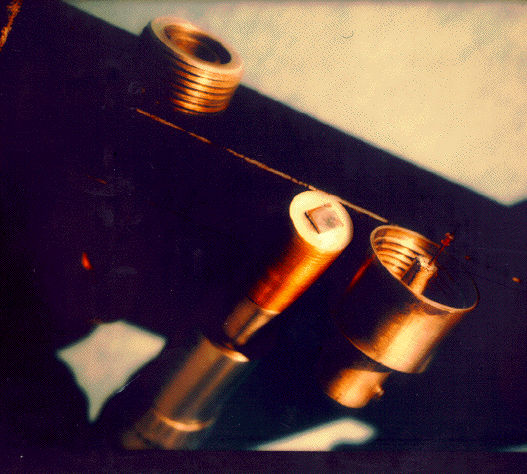
Figure 2: X-band waveguide oscillator set-up. The QWITT chip is mounted
on a micrometer post (left) and is wisker-contacted from the oppostie side
of the X-band waveguide (wisker mount on right).
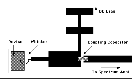
Figure 3: Planar microstrip circuit used to test QWITT diode oscillators.
To further study the QWITTs, an AlAs/GaAs DBRTD, two AlAs/GaAs QWITTs
(QWT I and QWT II), and an AlAs/InGaAs QWITT were also grown by molecular
beam epitaxy. A layer schematic diagram of the three AlAs/GaAs based quantum-well
structures is given in Fig. 4, where the layer thickness parameters W1,
W2, and W3 are varied for the three devices. For the DBRTD, which serves
as a baseline device, W1 = W3 = 0 Å and W2 = 100 Å. For QWT
I, W1 = 2000 Å, W2 = 100 Å , and W3 = 0 Å. For QWT II,
W1 = 0 Å, W2 = 200 Å, and W3 = 2000 Å. The fourth device
is an AlAs/InGaAs QWITT grown on an InP substrate where the quantum well
is formed by sandwiching a 47 Å In0.53Ga0.47As
well between 25 Å strained AlAs barriers. The quantum well is between
a symmetric layer profile consisting of 15 Å of undoped In0.53Ga0.47As
adjacent to the well followed by 1000 Å n- (8 x 1016cm-3)
In0.53Ga0.47As, and then 1000 Å of n+ (2 x 1018cm-3)
In0.53Ga0.47As.
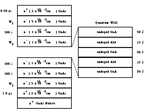
Fig. 4: Schematic cross section of the QWITT diode structures tested.
The I-V curves for the baseline DBRTD, the AlAs/GaAs QWITTs, and the AlAs/InGaAs
QWITT are shown in Fig. 5. Notice that ![]() has increased due to
the addition of a depleted drift region. Furthermore, the peak voltage for
QWT II is lower than that for QWT I, which should lead to a higher DC to
RF power conversion efficiency.
has increased due to
the addition of a depleted drift region. Furthermore, the peak voltage for
QWT II is lower than that for QWT I, which should lead to a higher DC to
RF power conversion efficiency.
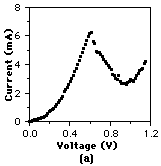
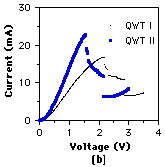
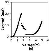
Fig. 5: I-V curves for the four device structures described as follows:
a) I-V curve for symmetric DBRTD (Area = 1.39 x 10⁻⁷ cm2)
b) I-V curves for QWT I (Area = 2.61 x 10⁻⁷ cm2) and
QWT II (Area = 3.34 x 10⁻⁷ cm2)
c) I-V curve for AlAs/InGaAs QWITT. (Area = 5.57 x 10⁻⁷ cm2)
For the QWITT diodes shown in Fig. 4, measurements were made using the microstrip
oscillator circuit (Fig. 3) and the same voltage source and multimeter as
in the DC measurements, but with the addition of a Tektronix 492A spectrum
analyzer to monitor RF oscillations. A summary of the experimental oscillator
results is given in Table III where the DC bias voltage in the NDR region
was adjusted until a maximum output power was obtained. For these measurements
the RF circuit was not intentionally designed to yield oscillations at any
particular frequency, although a large RF-to-ground bypass capacitor was
placed across the spectrum analyzer to suppress microwave oscillation, and
care was taken to prevent very low frequency DC bias line oscillation. Under
these conditions oscillations did still occur for all samples, at a frequency
between 250 - 500 MHz. No other attempts were made to tune the circuit.
All diodes produced an oscillation which had a very sharp spectrum (less
than 1 MHz bandwidth) and was stable for many hours. A major result is the
significant increase in output and efficiency from the AlAs/InGaAs QWITT,
mainly due to the suppression of a rapid rise in the current for voltages
beyond the valley point. The measured output power was compared to two types
of simple calculations for the maximum power available from these devices.
The first estimate for the maximum available power, given in the second
column of the table, is equal to (3/16) ![]() , which is correct ONLY
if the I-V curve is cubic in the negative differential resistance region
[9]. The second estimate is obtained by calculating, in the low frequency
limit, the time-averaged power (PAC), assuming a sinusoidal RF voltage swing
about a DC bias point, with the instantaneous current (I) taken from the
DC I-V curve evaluated at the total instantaneous voltage
, which is correct ONLY
if the I-V curve is cubic in the negative differential resistance region
[9]. The second estimate is obtained by calculating, in the low frequency
limit, the time-averaged power (PAC), assuming a sinusoidal RF voltage swing
about a DC bias point, with the instantaneous current (I) taken from the
DC I-V curve evaluated at the total instantaneous voltage ![]() . The maximum
power is found by numerically varying the bias voltage and RF swing. As
can be seen in Table III, the close match between this quasi-static calculation
and the measured results suggest that these devices are indeed delivering
their maximum available RF output power. Furthermore, the QWITT diodes,
as expected, deliver much more power than the simple DBRTD. Also, QWT II
and the AlAs/InGaAs QWITT exhibit very high DC-to-RF power conversion efficiencies.
. The maximum
power is found by numerically varying the bias voltage and RF swing. As
can be seen in Table III, the close match between this quasi-static calculation
and the measured results suggest that these devices are indeed delivering
their maximum available RF output power. Furthermore, the QWITT diodes,
as expected, deliver much more power than the simple DBRTD. Also, QWT II
and the AlAs/InGaAs QWITT exhibit very high DC-to-RF power conversion efficiencies.
The above method for comparing a device's expected power and actual output
at a low frequency allows easy determination of whether or not a circuit
for higher frequency operation should be designed and fabricated. In light
of this fact, QWT I was placed in an oscillator circuit that was iteratively
designed for 10 GHz operation, and an output power of 1.2 mW was obtained
at this frequency. For the AlAs/InGaAs QWITT, by simply removing the RF-to-ground
bypass capacitor from its circuit, the diode oscillation frequency increased
from about 250 MHz to about 3 GHz, while maintaining an output power of
over 2 mW. These are encouraging results, since for an oscillation frequency
increase of between 10 and 30 over the low frequency results, the output
power dropped by only a factor of about 2. Since no attempt has been made
to account for losses in the microstrip circuit, and no direct circuit tuning
was used, it is possible these diodes may actually produce nearly as much
power at 10 GHz as they did near 300 MHz. These output powers represent
the highest reported to date for quantum well oscillators.
Estimated Power (mW) |
Experimental Results | |||
| Device | Quasi- Static I-V Calculation | RF Power (mW) | RF Power Conversion Efficiency (%) | |
| QWD | 0.236 | 0.242 | 0.206 | 7.5 |
| QWT I | 1.55 | 2.60 | 2.66 | 8.5 |
| QWT II | 2.34 | 3.50 | 3.54 | 20.4 |
| InGaAs/AlAs QWITT | 4.59 | 4.87 | 4.79 | 29.2 |
We have presented dc and microwave characteristics of six different QWITT structures. A peak output power of more than 2 mW at 3 GHz from a single AlAs/InGaAs QWITT diode was obtained, and 1.2 mW at 10 GHz from a single AlAs/GaAs QWITT diode. At the date of these experiments, these were the highest output powers obtained from any quantum well oscillator at any frequency and were approximately five times higher power output than reported in the literature for a comparable frequency. No attempt was made to optimize either the microwave resonant cavity or the physical parameters of the diode to maximize the output power. Nonetheless, the performance achieved here suggests that through further improvements in device and circuit design higher power output may be possible. It seems clear that the actual power limitations of quantum well oscillators have not yet been determined, and that through the use of QWITT design principles useful power levels may be achieved at high millimeter wave frequencies.
1. E.R. Brown, W.D. Goodhue, and T.C.L.G. Sollner, J. Appl. Phys.,
64, pp. 1519-1529, Aug. 1988.
2. H. Gronqvist, A. Rydberg, H. Hjelmgren, H. Zirath, E. Kollberg, J. Soderstrom,
T. Andersson, Proc. of the 18th European Microwave Conference, pp. 370-375,
Stockholm, Sweden, Sep. 1988.
3. V.P. Kesan, D.P. Neikirk, B.G. Streetman, and P.A. Blakey, IEEE Elect.
Dev. Lett., EDL-8, pp. 129-131, April 1987.
4. V.P. Kesan, D.P. Neikirk, P.A. Blakey, and B.G. Streetman, and T.D. Linton,
IEEE Trans. on Elect. Dev., ED-35, pp. 405-413, April 1988.
5. V.P. Kesan, T.D. Linton, C.M. Maziar, D.P. Neikirk, P.A. Blakey, and
B.G. Streetman, 1987 IEEE International Electron Device Meeting Tech. Dig.,
pp. 62-65, Dec. 6-9, 1987.
6. D.R. Miller, V.P. Kesan, R.L. Rogers, C.M. Maziar, and D.P. Neikirk,
Proc. of the 13th Int. Conf. on Infrared and Millimeter Waves, Dec. 1988.
7. I. Song and D.S. Pan, IEEE Elect. Dev. Lett., EDL-8, pp.
560-562, Dec. 1987.
8. V.P. Kesan, A. Mortazawi, D.R. Miller, V.K. Reddy, D.P. Neikirk, and
T. Itoh, "Microwave and Millimeter Wave QWITT Diode Oscillators,"
IEEE Trans. Microwave Theory Tech. MTT-37 , Dec. 1989, pp. 1933-1941.
9. W. F. Chow, Principles of Tunnel Diode Circuits: Wiley, 1964.