also see:
V.P. Kesan, A. Mortazawi, D.R. Miller, T.Itoh, B.G. Streetman, and D.P.
Neikirk, "Microwave Frequency Operation of the Quantum Well Injection
Transit Time (QWITT) Diode," Electronics Letters 24, 24 Nov.
1988, pp. 1473-1474.
V.P. Kesan, A. Mortazawi, D.R. Miller, V.K. Reddy, D.P. Neikirk, and T.
Itoh, "Microwave and Millimeter Wave QWITT Diode Oscillators,"
IEEE Trans. Microwave Theory Tech. MTT-37, Dec. 1989, pp. 1933-1941.
S. Javalagi, V. Reddy, K. Gullapalli, and D. Neikirk, "High efficiency
microwave diode oscillators," Electronics Letters 28, 27 August
1992, pp. 1699-1701.
also see our work on the theoretical behavior of double barrier resonant tunneling diodes with spacer layers:
Influence of Space Charge
and Quantum Well Negative Resistances on Resonant Tunneling Diodes
and our experimental work on various QWITT diodes:
Experimental Operation of the Quantum Well Injection Transit Time (QWITT) Diode
High Power and High Efficiency Quantum Well Diode Microwave Oscillators
Shiva Javalagi, Vijay Reddy, Kiran Gullapalli, and Dean Neikirk
Department of Electrical and Computer Engineering
The University of Texas at Austin
Abstract
Microwave oscillators using quantum well injection transit (QWITT) diodes have produced CW output powers of 20 mW with DC to RF conversion efficiencies as high as 50%. Oscillation frequency and power are in good agreement with large signal RF device simulations. The models should allow device and circuit design for even higher output power and higher frequencies of oscillation.
Summary: Double barrier resonant tunnelling diodes (DBRTDs) have
been extensively investigated for use as high frequency sources. However,
a major drawback of DBRTDs has been their low output power. Output power
in negative differential resistance devices is proportional to the maximum
current and voltage swings in the NDR region. The motivation for the quantum
well injection transit (QWITT) diode is that the voltage and current differences
between the peak and the valley, ![]() and
and ![]() , respectively,
must be made as large as possible to increase output power. In the QWITT
diode
, respectively,
must be made as large as possible to increase output power. In the QWITT
diode ![]() is increased through the inclusion of a depleted drift
region, while
is increased through the inclusion of a depleted drift
region, while ![]() is determined by the quantum well injector. This increases
both the specific negative resistance and the maximum output power of the
device. The QWITT's higher specific negative resistance also allows easier
matching between RF circuits and large area diodes, while avoiding low frequency
bias line oscillations. In this paper we present DC and RF data for two
InGaAs/AlAs QWITT diodes with 120 nm and 180 nm depletion region lengths.
The 180 nm device produced a single device output power of 20 mW without
requiring any device heat sinking or substrate thinning. In addition, DC
to RF conversion efficiency as high as 50 % was obtained under optimum RF
circuit / device matching conditions.
is determined by the quantum well injector. This increases
both the specific negative resistance and the maximum output power of the
device. The QWITT's higher specific negative resistance also allows easier
matching between RF circuits and large area diodes, while avoiding low frequency
bias line oscillations. In this paper we present DC and RF data for two
InGaAs/AlAs QWITT diodes with 120 nm and 180 nm depletion region lengths.
The 180 nm device produced a single device output power of 20 mW without
requiring any device heat sinking or substrate thinning. In addition, DC
to RF conversion efficiency as high as 50 % was obtained under optimum RF
circuit / device matching conditions.
Two InGaAs/AlAs QWITT diodes with drift region lengths 180 nm and 120 nm, referred to as QWITT 1 and QWITT 2, were grown on an n-type InP substrate using molecular beam epitaxy. The layer schematic of the diodes is shown in Figure 1. The quantum well is formed by sandwiching a 4.7 nm In0.53Ga0.47As layer between 2.5 nm strained AlAs layers. The quantum well is between a symmetric layer profile consisting of 1.5 nm of undoped In0.53Ga0.47As adjacent to the barriers followed by about 10 nm n (2.3 x 1016 cm-3) In0.53Ga0.47As and 10 nm n (1.3 x 1017 cm-3) In0.53Ga0.47As. The drift region is placed below the quantum well. Standard processing techniques were used to fabricate mesa isolated diodes with Au topside contacts. The room temperature current density measured on these devices was about 8 kA/cm2 and the peak to valley current ratio (PVCR) was about 20. Current density versus voltage characteristics of both diodes are shown in Figure 2.
Two resonator circuits were designed using 50 ohm microstrip lines, as shown in Figure 3. The design is based on Kurokawa's oscillation criterion (i.e. Zdevice = -Zcircuit) [1]. Both small signal and large signal calculations on the QWITT diodes show a very nearly real impedance for low microwave frequencies (< 5 GHz). The open circuit stub in the circuit produces a real impedance at the device only over a narrow band of frequencies; thus the Kurokawa condition can be satisfied only in this frequency band. For the stub lengths chosen oscillation should occur at about 1 and 2.7 GHz for circuits 1 and 2, respectively. Since the diode impedance is nearly real, the frequency of the oscillation is expected to be independent of the diode structure (i.e QWITT 1 or QWITT 2) and area. These simple circuit configurations were chosen to verify the large signal model and performance of the QWITT diodes at microwave frequencies.
The RF output power was measured by placing each sample at the end of the circuit and varying the DC bias voltage until maximum output power was obtained. Contact to mesas was made by a tungsten whisker at the end of the circuit. Different areas on each sample were also probed. Stability of the QWITT oscillators was very good, producing a sharp spectrum with a linewidth of about 5-10 kHz, measured on a high resolution HP8567 Spectrum Analyzer. The experimental results for both QWITT I and QWITT II operating in the two circuits are shown in Table I. A DC-RF power conversion efficiency as high as 50 % has been achieved with a power density of 4 kW/cm2 at 2.4 GHz. To our knowledge, this is the best efficiency ever measured in continuous wave operation for a two terminal device. Conventional IMPATT diodes have been shown to have efficiencies of 60%, but only in a pulsed operation mode [2]. In continuous operation IMPATTs have demonstrated efficiencies only as high as 43% [3]. Gunn diodes typically have DC to RF conversion efficiencies of less than 10% [4].
The highest power output of 21 mW was attained without requiring any special heat sinking mechanism. This is the highest power output reported to date for a quantum well diode oscillator. Such high power is possible since these QWITT diodes have very high specific negative resistance, allowing the use of very large area diodes without producing bias line oscillation.
Quasi-static IV calculations were performed by numerically varying the RF voltage swing at different bias points in the NDR region, using the stabilized DC IV curves for both diodes. The results obtained in Table I are consistent with the large signal analysis performed on the stabilized DC IV curves. At optimum bias and RF voltage swing, the large signal calculations on QWITT 1 yield a power density of 4.1 kW/cm2 with DC to RF conversion efficiency of 40 %, while QWITT 2 gives 3.0 kW/cm2 at 43 % efficiency. Since the large signal specific negative resistance of the device is a strong function of the RF amplitude, the RF voltage swing necessary to satisfy the Kurokawa condition changes with device area. Hence the power density varies with the area for a fixed RF circuit. The variation of measured power density with device area was fully consistent with the behavior predicted by our models.
To extend performance to higher frequencies a more accurate large signal analysis is necessary. A large signal, time-dependent drift-diffusion model was used to characterize these diodes at high frequencies. Calculated frequency versus power curves for QWITT 1 and QWITT 2 are shown in Figure 4. To verify the model, QWITT 1 was also tested in a 10 GHz microstrip resonator circuit. With an unoptimized circuit, the DC-RF conversion efficiency was 20% with a power density of 1.7 KW/cm2 at 9.67 GHz. Higher current density is desirable for higher microwave frequency operation. Hence new device designs including thinner quantum well barriers to increase current density, and larger drift lengths for higher specific negative resistance, are being investigated to extend the performance of these QWITT diodes.
References
1. K. Kurokawa, "Some basic characteristics of broadband negative resistance oscillator circuits," Bell Systm. Tech. J. 48, July 1969, pp. 1937-1955.
2. K. Chang, "Avalanche diodes as UHF and L-band sources," RCA Review, Vol. 30, 3, 1969.
3. D.E. Iglesias, and W.J. Evans, "High-efficiency CW IMPATT operation," Proc. IEEE, Vol. 56, 1610, 1968.
4. F.B. Frank, and G.F. Day, "High CW power K-band Gunn oscillators,"
Proc. IEEE, Vol. 57, 339, 1969. 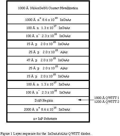
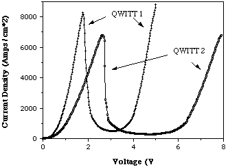
Figure 2: Stabilized DC-IV curves for QWITT 1 and QWITT 2.
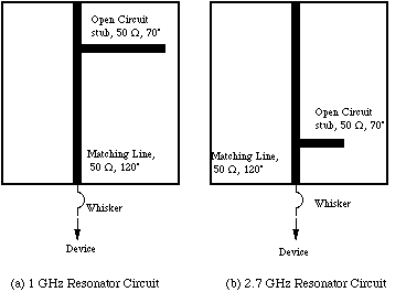
Figure 3: Microstrip circuits used for microwave testing of InGaAs/AlAs QWITT diodes.
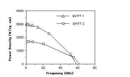
Figure 4: Large-signal calculated power density characteristics for QWITT 1 and QWITT 2.
Sample: InGaAs/AlAs |
Area (10-8/cm2) |
Frequency (GHz) (circuit I) |
Power Density (KW/cm2) (circuit I) |
Efficiency % (circuit I) |
Frequency (GHz) (circuit II) |
Power Density (KW/cm2) (circuit II) |
Efficiency % (circuit II) |
|---|---|---|---|---|---|---|---|
QWITT I (W=1800Å) |
1250 | 0.908 | 1.65 | 11 | NM* | NM* | NM* |
QWITT I (W=1800Å) |
300 | 0.941 | 3.90 | 42 | 2.380 | 3.6 | 39 |
QWITT I (W=1800Å) |
160 | 0.951 | 2.85 | 39 | 2.313 | 4.0 | 44-50 |
QWITT I (W=1800Å) |
68 | 0.953 | 2.40 | 27 | 2.448 | 2.8 | 36 |
QWITT II (W=1200Å) |
300 | 0.943 | 2.60 | 35 | 2.238 | 1.5 | 20 |
QWITT II (W=1200Å) |
144 | 0.930 | 3.00 | 37 | 2.320 | 2.2 | 26 |
QWITT II (W=1200Å) |
68 | 0.947 | 2.40 | 35 | 2.357 | 1.7 | 24 |
NM* Not Measured
Table I. Power Density & DC to RF conversion efficiency results for QWITT I and QWITT II.