The University of Texas at Austin
For further information contact Professor Dean Neikirk
at
neikirk@uts.cc.utexas.edu
Please see our complete papers on this topic:
S. M. Wentworth, D. P. Neikirk, and C. R. Brahce, "High Frequency Characterization
of Tape-Automated Bonding (TAB) Interconnects," SPIE Advances in Semiconductors
and Superconductors: Physics and Device Applications, Conf. 947: Interconnection
of High Speed and High Frequency Devices and Systems, Newport Beach, CA,
March 13-18, 1988, pp. 81-84.
S. M. Wentworth, D. P. Neikirk, and C. R. Brahce, "The high frequency
characteristics of Tape Automated Bonding (TAB) interconnects," IEEE
Trans. Components, Hybrids, and Manufacturing Tech., vol. 12, pp. 340-347,
1989.
- ABSTRACT
- 1. INTRODUCTION
- 2. HIGH FREQUENCY MODELING OF TAB TAPE
- 3. MICROWAVE CHARACTERIZATION
- 4. RECOMMENDED DESIGN
- 5. CONCLUSIONS
- 6. ACKNOWLEDGMENTS
- 7. REFERENCES
- Figures
ABSTRACT
The geometry of tape automated bonding (TAB) tape lends itself to microwave
packaging applications where high density signal lines are required. In
this paper we model the tape as a transmission line, since above 5 GHz the
tape length is significant compared to the signal wavelength. A test chip
has been fabricated to allow determination of the microwave characteristics
of 3M's 120 lead, two-layer gold-plated ED copper tape, which has a polyimide
support layer and an inner lead pitch of 8 mils. A characteristic impedance
of 100 +/- 10 Ohms is found for the tape based upon measurements up to 18
GHz. This compares well with the theoretical model, which predicts an impedance
between 98 and 118 Ohms. Theoretical models and practical considerations
have been used to design a TAB tape which should be impedance matched to
50 Ohms and exhibit good signal isolation. This design is presented, and
the tape is currently being manufactured.
1. INTRODUCTION
With the advent of very high speed integrated circuits (VHSIC) and monolithic
microwave and millimeter wave integrated circuits (MIMIC) there is an increasing
demand for packages which can operate at high frequencies. For example,
present MIMIC packaging for digital applications can handle up to 4 GHz
clock rates with 24 RF I/Os [1]. In contrast, for analog applications the
number of I/O's is usually low, but each line must operate at very high
frequency; typical high density packages may have up to 8 RF I/Os operating
at 18 GHz [2]. Some applications may require a higher number of I/O's with
very large bandwidth. One such analog device which would require many RF
connections is a monolithic millimeter wave imaging array [3,4].
One possible technique to achieve high density interconnects for high frequency
applications would be through the use of tape automated bonding (TAB) tape.
The particular tape used in this study is 120 lead, two-layer gold-plated
ED copper tape with a polyimide support layer and an inner lead bond (ILB)
pitch of 8 mils.
For MIMIC applications frequencies much higher than 5 GHz are of interest.
Therefore, in this paper the TAB interconnects will be treated as transmission
lines rather than lumped elements. The results of measurements between 90
MHz and 18 GHz on 120 lead TAB tape will be compared with a theoretical
model, and a new TAB tape design for very high frequency applications will
be recommended.
2. HIGH FREQUENCY MODELING OF TAB TAPE
A crucial requirement for systems utilizing MIMIC technology is
the provision for efficient signal transmission throughout the system. To
achieve this, both the chips and the PCBs use impedance-controlled transmission
line circuits. Since the TAB interconnect studied here is about one half
wavelength long at 10 GHz, a transmission line model is also necessary for
the interconnects between PCB and chip.
The TAB tape conductors are approximately 1.4 mils thick and are supported
by a thin (2 mil) layer of polyimide. For this tape configuration, at very
high frequencies (such as the microwave frequencies used here) every other
lead must be grounded to provide signal isolation and impedance control.
With adjacent lines grounded, the TAB tape resembles coplanar waveguide
(CPW) [5] . CPW is one of several types of planar waveguide which have proven
to be broadband [6], and which finds application in MIMIC chips.
A conformal mapping technique can be used to calculate the characteristic
impedance and effective dielectric constant of CPW with finite dimensions
[7]. A modification to this technique considers the effect of conductor
thickness. The resulting equations are

(1)
and 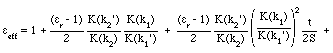

(2)
where

(3)
and
(4)
with the values a, b, c, and h as given in Fig. 2 of reference 12. K(f)
/ K(f') is a ratio of complete elliptical integrals of the first kind. This
ratio can be estimated using Hilberg's approximation [8], which is given
in general form as
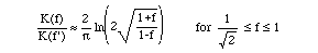
(5a)
and
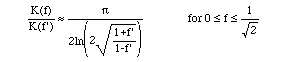
(5b)
where  . This approximation has been found to agree well with tabulated
values of (K(f) / K(f') over our range of interest (0.0200 < f < .9998).
. This approximation has been found to agree well with tabulated
values of (K(f) / K(f') over our range of interest (0.0200 < f < .9998).
For the TAB tape used in this study, the TAB tape conductor width is 4 mils
with an 8 mil pitch at the inner lead bond area. These leads flair out to
an 8 mil wide conductor with a 16 mil pitch. The copper conductor thickness
is nominally 1.4 mils, plated with a thin (nominally 20 uinches) layer of
gold. Beneath most of the tape is a 2 mil thick polyimide layer of relative
dielectric constant 3.6. Using these values in the above equations, the
characteristic impedance is found to range from 98 Ohms at the inner lead
end to 118 Ohms at the outer lead end. The wide pitch end of the tape is
about twice as long as the narrow pitch end.
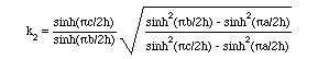
Additional signal isolation can be achieved by placing a ground plane underneath
the polyimide layer of the tape. With this ground plane added, the tape
is best modeled by conductor-backed coplanar waveguide (CBCPW). The CBCPW
is a microstrip/CPW hybrid which has also been modeled using a conformal
mapping approach [9]. For the mapping used in this technique the ground
planes adjacent to the central conductor must be considered infinite. An
additional capacitance term to consider conductor thickness can be included
with the equations given by Ghione and Naldi [9] to obtain
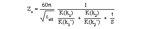
(6)
where k1 and k1' are given as before. The term k2 is given by
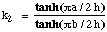
(7)
and  . The effective dielectric constant
  is given by
(8)
The Hilberg approximation is again used to determine the elliptic ratios.
3. MICROWAVE CHARACTERIZATION
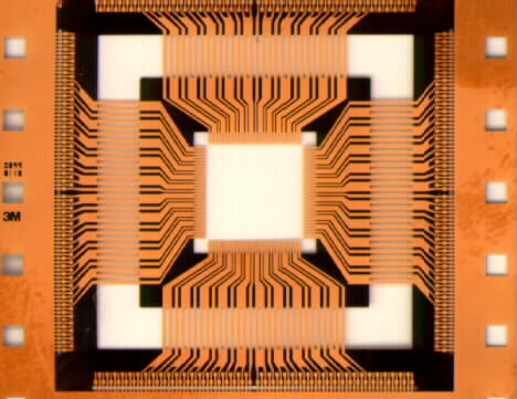
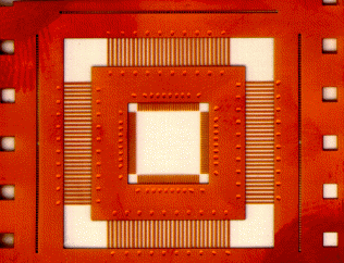
A test chip has been fabricated to allow determination of TAB tape
microwave characteristics. Fig. 1 shows a photomicrograph of the chip which
contains a short-to-ground, an open, 8 resistors, and a through coplanar
waveguide. The resistors and ground plane were made by resistance heated
evaporation of chromium and gold, respectively, using a lift-off technique
[10].
The inner lead bonds of the TAB tape were made to electroplated gold bumps
of about 10um height. The outer lead bonds were made to a copper clad printed
circuit board (PCB) which has been plated with gold to facilitate bonding.
The PCB is a microwave laminate of dielectric constant er=10.5, with 1/2
oz. electrodeposited copper cladding on both sides. The dimensions of the
CBCPW were chosen to obtain a 50 Ohms line, based on equations of Ghione
and Naldi [9], which have been verified experimentally.
All of the microwave testing of the TAB tape was performed with an HP8510
Network Analyzer. The 8510 was connected to the chip, tape, and board through
an OSM plug-to-7mm connector and OSM coaxial jack launcher, as shown in
Fig. 2. For measurements of Zo and vp the network analyzer was operated
in the time domain low pass mode to simulate a time domain reflectometry
(TDR) measurement [11]. The frequency domain response was taken from 90
MHz to 18 GHz and Fourier transformed to the time domain.
Estimation of the TAB tape propagation velocity vp is complicated by the
HP8510's system response time, which is 55 psecs for an 18 GHz bandwidth,
compared to an approximate 80 psec round-trip traversal time for the tape.
The tape length was measured as 6.6 mm, so the experimentally determined
vp is 0.55c. Using the relation vp = c /  , the effective dielectric
constant for the tape is 3.3. This value is rather high considering
that the theory (eq.2) predicts an of 1.8 at the wide end of the tape
and 2.7 at the narrow end, corresponding to a vp range of from 0.7c to 0.6c.
, the effective dielectric
constant for the tape is 3.3. This value is rather high considering
that the theory (eq.2) predicts an of 1.8 at the wide end of the tape
and 2.7 at the narrow end, corresponding to a vp range of from 0.7c to 0.6c.
The characteristic impedance Zo was estimated using the Hewlett-Packard
Circuit Modeling Program (CMP) in conjunction with the network analyzer.
The CMP will determine the S-parameters for a circuit containing up to 200
nodes, including transmission lines, resistors, capacitors, and inductors.
These S-parameters are transferred to the 8510 where a time domain low pass
response is obtained and compared to the actual response.
Although our theoretical models suggest a change of impedance from the wide
end to the narrow end of the tape, we modeled the TAB tape as a transmission
line with a single characteristic impedance. It is impractical to break
up the tape into sections since the analyzer cannot resolve lengths this
short.
Values of Zo were inserted into the transmission line model to obtain the
best fit with the data. On some lines, the value of the terminating resistance
was considerably different from the characteristic impedance of the tape
(i.e. R = 155 Ohms). On these lines, the response of the TAB tape was completely
hidden by the slower system response. Only on lines with a terminating resistance
of value close to the TAB tape impedance was a measurement possible. With
a terminating resistance of 114 [[Omega]], the Zo for the TAB tape was found
to be about 100 [[Omega]]. The estimated TAB tape impedance of 100 +/- 10
Ohms compares reasonably well with the theoretical range of 98 to 118 Ohms
predicted by our model.
Preliminary measurements of cross-talk and loss in the TAB tape have also
been performed. Initial results suggest the cross-talk is less than -30
dB at 10 GHz, and loss is no greater than -2 dB for frequencies less than
8 GHz.
4. RECOMMENDED DESIGN
Conventional transmission lines on MIMIC chips and microwave PCB
have characteristic impedances of 50 Ohms or 75 Ohms. Clearly, a tape impedance
of 100 Ohms does not match well with these values. However, theoretical
as well as practical considerations may be used to design a TAB tape with
an impedance of 50 Ohms and good signal isolation. In such a design, a ground
plane is placed beneath the thin dielectric layer. This has the dual benefits
of reducing the characteristic impedance and improving signal isolation.
Further isolation is achieved by placing wide ground strips between each
signal line, which are connected to the underlying ground plane by vias.
The method of Ghione and Naldi [9] modified by a consideration of conductor
thickness, can be used to design a 50 Ohms line (eqns. 6-8). Figures 3-4
show such a two layer TAB tape designed to produce a controlled impedance
of 50 Ohms.
5. CONCLUSIONS
We have modeled the TAB tape as a CPW transmission line with finite dimensions.
The model predicts the impedance of 120 lead tape as 98 to 118 [[Omega]].
This compares reasonably well with experiment, which found an impedance
of 100 +/- 10 [[Omega]] for the TAB tape. Improved isolation and lower impedance
can be achieved by adding a ground plane beneath the polyimide support layer
and separating the signal lines by wide ground strips. A theoretical model
has been used to design a 50 [[Omega]] TAB tape for MIMIC applications.
6. ACKNOWLEDGMENTS
The authors would line to acknowledge valuable discussions with P. Cheung,
B. Parizek, J. Woolley, H. Hoenisch, and D. Behm. This research was supported
by a grant from 3M Corporation.
7. REFERENCES
1. D. H. Smith, T. G. Bowman, R. Lind, and T. S. Riley, "New Approaches
to Packaging for High Speed GaAs IC Applications," 1985 GaAs IC
Symposium Technical Digest, pp.151-154.
2. G. Herrick and K.E. Jones, "Surface-Mount Pack Houses GaAs MMICs,"
Microwaves & RF, pp.157-169, June 1986.
3. C. Zah, D. Kasilingam, J. S. Smith, D. Rutledge, "Millimeter Wave
Monolithic Schottky Diode Imaging Arrays," Int. J. Infrared and
Millimeter Waves, Vol. 6, No.10, pp.981-997, 1985.
4. D. B. Rutledge, D. P. Neikirk, D. Kasilingam, "Integrated Circuit
Antennas," in Infrared and Millimeter Waves, Vol. 10 (K. J.
Button, ed., Academic Press, New York, 1983).
5. C. P. Wen, "Coplanar Waveguide: A Surface Strip Transmission Line
Suitable for Nonreciprocal Gyromagnetic Device Applications," IEEE
Trans., MTT-17, No.12, pp.1087-1088, Dec.1969.
6. M. V. Schneider, "Microstrip Lines for Microwave Integrated Circuits,"
BSTJ, pp.1421-1444, Dec.1968.
7. C. Veyres, V. F. Hanna, "Extension of the application of conformal
mapping techniques to coplanar lines with finite dimensions," Int.
J. Electronics, Vol. 48, No.1,pp.47-56, 1980. (one equation is not correct)
8. W. Hilberg, "From approximations to exact relations for characteristic
impedances," IEEE Trans. Microwave Theory Tech., Vol MTT-17, No. 5,
pp.259-265, May 1969.
9. G. Ghione, C. Naldi, "Parameters of Coplanar Waveguide with Lower
Ground Plane," Electronics Letters, Vol.19, No.18 , pp.734-735,
Sept. 1, 1983.
10. R. Halverson, M. MacIntyre, W. Motsiff, "The Mechanism of Single-Step
Liftoff with Chlorobenzene in a Diazo-Type Resist," IBM J. Res.
Develop., Vol.26, pp.590-594, 1982.
11. HP 8510 Network Analyzer System Operating and Programming Manual,
Hewlett-Packard Company, 1985.
12. S. M. Wentworth, D. P. Neikirk, and C. R. Brahce, "High Frequency
Characterization of Tape-Automated Bonding (TAB) Interconnects," SPIE
Advances in Semiconductors and Superconductors: Physics and Device Applications,
Conf. 947: Interconnection of High Speed and High Frequency Devices and
Systems, Newport Beach, CA, March 13-18, 1988, pp. 81-84.
Figures
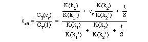
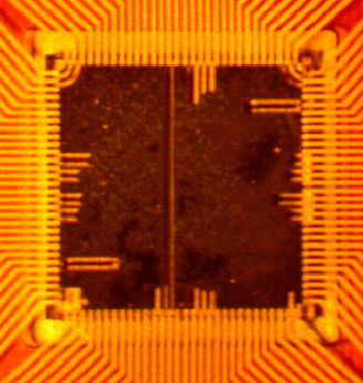 Fig. 1. TAB test chip design for determination of microwave
characteristics.
Fig. 1. TAB test chip design for determination of microwave
characteristics.
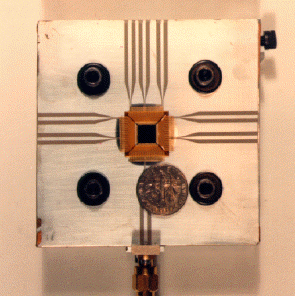 Fig. 2. The microwave test assembly. An OSM coaxial jack launcher
and an OSM plug-to-7mm connector is used to connect the HP8510 to the PCB
upon which the TAB tape is outer lead bonded.
Fig. 2. The microwave test assembly. An OSM coaxial jack launcher
and an OSM plug-to-7mm connector is used to connect the HP8510 to the PCB
upon which the TAB tape is outer lead bonded.
 Close up of test chip connected to board via TAAB tape.
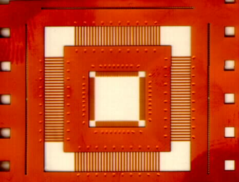
Fig. 3. Recommended tape design for high frequency MIMIC applications. It
features a grounded backplane which is connected to the wide topside ground
lines by two vias per line, and optimum CBCPW design for 50 Ohms.
Life size photo of 50 ohm TAB tape, front 
 enlargement
of tape front; click image for JPEG high res scan.
enlargement
of tape front; click image for JPEG high res scan.
life size photo of 50 ohm TAB tape, back 
 enlargement
of tape back; click image for JPEG high res scan.
enlargement
of tape back; click image for JPEG high res scan.
If you support pict files, click here
for a big (400+ K), detailed image of the front side of the 50 ohm tape.
If you support pict files, click here for
a big (400+ K), detailed image of the back side of the 50 ohm tape.