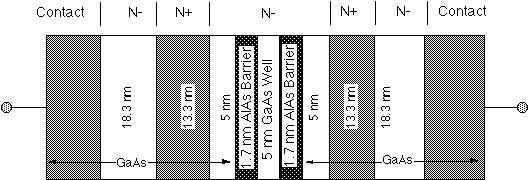
 Figure 1:
Multi-state device using a symmetric N-N+-N spacer layer / AlAs
barrier / GaAs quantum well / AlAs barrier / N-N+-N spacer layer
structure.
Figure 1:
Multi-state device using a symmetric N-N+-N spacer layer / AlAs
barrier / GaAs quantum well / AlAs barrier / N-N+-N spacer layer
structure.
Observation of Zero-Bias Multi-State Behavior in Selectively Doped
Two-Terminal Quantum Tunneling Devices
K. K. Gullapalli, A. J. Tsao, and D. P. Neikirk
Microelectronics Research Center
The University of Texas at Austin, Austin, TX 78712
A more complete discussion of this material can be found in our publications:
We have designed and demonstrated a quantum tunneling diode that exhibits multiple I-V curves persistent across zero bias [1]. Based on a self-consistent quantum tunneling calculations, we have found multiple conduction states in diodes that combine a heterobarrier with an N-N+-N spacer layer [2-4]. We have experimentally observed multiple stable I-V curves in such a device grown in the GaAs/AlAs material system using molecular beam epitaxy [5]. Each state produces a distinct terminal device impedance that is persistent at zero bias. The device can be repetitively switched between the states by the application of an appropriate threshold voltage. The device maintains memory of its state even under short circuit conditions.
The multiple conduction state phenomena have been observed in several different device structures we fabricated with N-N+-N spacer layers in combination with AlAs/GaAs quantum wells. A schematic of one such device is shown in Fig. 1. The device structure was grown in a Varian Gen II MBE system. The double barrier quantum well structure consists of an 18 monolayer (ML) lightly doped N-type (1015 cm-3) GaAs quantum well sandwiched between nominally symmetric 6 ML unintentionally doped AlAs barriers. The quantum well structure is surrounded on both sides by an 18 ML N-type (1015 cm-3) GaAs layer, 43 ML N+ (4x1018cm-3) GaAs layer, and 65 ML N (1015 cm-3) GaAs layer. Crucial to the device operation is the doping sequence in the spacer layers. We emphasize that only the devices with the doping scheme in Fig. 1 have shown evidence of multiple conduction curves, both in our models and our experiments.
The measured room temperature I-V characteristics of the diode are shown in Figure 2. The calculated I-V characteristic at 300K is shown in Figure 3. Note that the calculation results in three conduction branches (states A, B, and C), two of which (B and C) are mirror images of each other. We have also observed three conduction branches in experiment. Figure 2 shows the two most dominant states we have repetitively observed. The device possesses memory, in that once the device is placed in one state it will remain in that state over a wide range of bias voltage. In particular, the multiple states exist even at zero bias. Once the device is placed on one branch of its I-V characteristic, it will remain on that branch even under short circuit conditions.
That the device retains memory of the conduction branch it lies on, even after short circuiting, can be understood by examining the zero bias self-consistent potential profile corresponding to the different conduction states. The solutions were obtained by self-consistently solving the Schrödinger and Poisson equations. Shown in Figures 4, 5, and 6 are conduction band edges and the corresponding electron concentrations for the different states at zero bias. State A reflects the structural symmetry of the device about the center of the quantum well. The other two solutions are asymmetric and are mirror images of each other about the center of the quantum well. In the asymmetric states, the electron concentration in one of the heavily doped layers adjacent to the heterostructure is much lower than that in the symmetric state. The reduced charge is compensated mainly by a higher electron concentration in the outer undoped layers. All three solutions satisfy space charge neutrality. The stability of each state is the result of the large differences in the electron concentration very close to the heterobarrier structure.
The device operation is very robust. We have observed memory for a duration of several minutes under both short circuit and open circuit conditions, and have not observed any spontaneous transitions between states while holding the device at zero bias. Our simulations have also predicted similar behavior in diodes based on single barriers. Although it appears that a double barrier quantum well is desirable we expect this phenomena to occur in other heterostructure devices in conjunction with suitably doped spacer layers. Both hole-based and electron-based devices should be possible through the use of proper doping and band offsets. III-V as well as IV-IV (i.e., silicon - germanium) compound semiconductors should be suitable for use in this device structure.
This device has the potential to provide memory for high speed electronic systems. In addition, the area and thickness required for the device structure is very small, yielding the possibility of very high density. One shortcoming of compound semiconductors for integrated circuit applications has been the lack of a good memory cell; the device proposed here may provide this critical component.
References
1. K. K. Gullapalli, A. J. Tsao, and D. P. Neikirk, "Observation of zero-bias multi-state behavior in selectively doped two-terminal quantum tunneling devices," IEEE International Electron Devices Meeting, San Francisco, CA, Dec. 13-16, 1992, pp. 479-482.
2. K. K. Gullapalli, A. J. Tsao, and D. P. Neikirk, "Multiple self-consistent solutions at zero bias and multiple conduction curves in quantum tunneling diodes containing N- - N+ - N- spacer layers," Appl. Phys. Lett., vol. 62, pp. 2971-2973, 1993.
3. K. K. Gullapalli, D. R. Miller, and D. P. Neikirk, "Wigner-Poisson simulation of memory switching heterostructure tunneling diodes," IEEE International Electron Devices Meeting, Washington, DC, Dec. 5-8, 1993, pp. 109-112.
4. K. K. Gullapalli, D. R. Miller, and D. P. Neikirk, "Simulation of quantum transport in memory-switching double-barrier quantum-well diodes," Phys. Rev. B, vol. 49, pp. 2622-2628, 1994.
5. K. K. Gullapalli, A. J. Tsao, and D. P. Neikirk, "Experimental observation of multiple current - voltage curves and zero-bias memory in quantum well diodes with N- - N+ - N- spacer layers," Appl. Phys. Lett., vol. 62, pp. 2856-2858, 1993.
Figure 1:
Multi-state device using a symmetric N-N+-N spacer layer / AlAs
barrier / GaAs quantum well / AlAs barrier / N-N+-N spacer layer
structure.
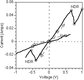 Figure 2:
Measured room temperature I-V curve of multi-state N-N+-N spacer
layer / AlAs / GaAs quantum well combination shown in Fig. 1. Only the two
most stable curves are shown. Arrows indicate bias ranges over which no
transitions between states have been observed.
Figure 2:
Measured room temperature I-V curve of multi-state N-N+-N spacer
layer / AlAs / GaAs quantum well combination shown in Fig. 1. Only the two
most stable curves are shown. Arrows indicate bias ranges over which no
transitions between states have been observed.
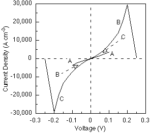
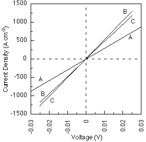
Figure 3: Calculated room temperature current density versus voltage curve for the device shown in Fig. 1. In the calculation the N+ layers were assumed to be 1018 cm-3, and the lightly doped layers to be 1015 cm-3. The three self-consistent solutions are labeled State A, State B, and State C.
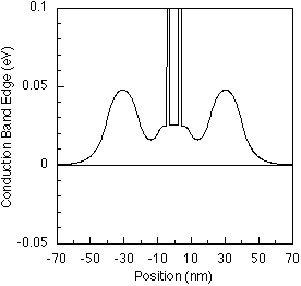
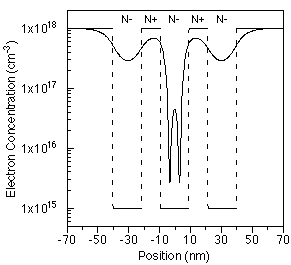
Figure 4: Calculated self-consistent conduction band edge and electron concentration for State A; band edge offset of the AlAs barriers is taken to be 1.05 eV.
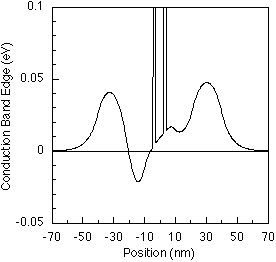
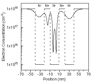
Figure 5: Calculated self-consistent conduction band edge and electron concentration for State B; band edge offset of the AlAs barriers is taken to be 1.05 eV.
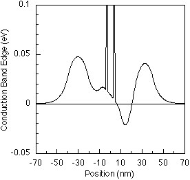
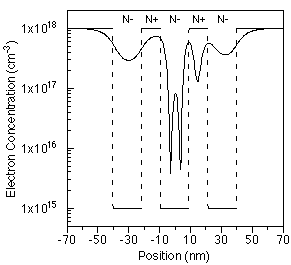
Figure 6: Calculated self-consistent conduction band edge and electron concentration for State C; band edge offset of the AlAs barriers is taken to be 1.05 eV.