For complete details, please see our publication:
Youngmin Kim and Dean P. Neikirk, "Design for Manufacture of Micro
Fabry-Perot Cavity-based Sensors," Sensors and Actuators A 50, Jan.
1996, pp. 141-146.
Design for Manufacture of Micro Fabry-Perot Cavity-based Sensors
Youngmin Kim and Dean P. Neikirk
Microelectronics Research Center
Department of Electrical and Computer Engineering
The University of Texas at Austin
Austin, TX 78712
- Abstract
- Introduction
- Model
- Example Designs
- Conclusions
- References
Abstract
Currently, the operation of a number of sensors is based on the measurement
of the optical path length of a micro-Fabry-Perot cavity. In this paper
we consider the impact of manufacturing errors on the performance of such
sensors, and discuss designs that minimize the impact of these variations.
In particular, we consider how random errors in thickness of the cavity
mirrors influence the accuracy with which gap can be measured. We find that
an optimum combination of initial gap and mechanical travel of the cavity
exists for a given mirror design that gives the least variation in response
curve. Designs that maximize the manufacturing yield of Fabry-Perot sensors
made with micromachining techniques are also discussed.
Introduction
Fabry-Perot cavity-based sensors have been widely used for their versatility;
for example they have been used to sense both pressure and temperature [1-4].
This kind of sensor detects changes in optical path length induced by either
a change in the refractive index or a change in physical length of the cavity.
Using micromachining techniques miniature Fabry-Perot sensors have recently
been proposed and fabricated [1, 4, 5]. Micromachining techniques make Fabry-Perot
sensors more attractive by reducing the size and the cost of the sensing
element. Another advantage of the miniature Fabry-Perot sensor is that low
coherence light sources, such as light emitting diodes (LEDs), can be used
to generate the interferometric signal, since the optical length of the
miniature cavity is of the same order as the wavelength of the light, and
shorter than the coherence length of a typical LED.
In these devices the cavity mirrors can be either dielectric layers or metal
layers deposited or evaporated during the manufacturing process. The thickness
of each layer must be tightly controlled to achieve the target performance
of a sensor. However, there are unavoidable errors in thickness even though
techniques of thickness control for thin films have rapidly improved [6].
For Fabry-Perot optical interference filters it has long been
recognized that the performance of the filter is greatly influenced by random
thickness variations in the films used [7, 8].
In this paper, we consider a Fabry-Perot "gap" sensor which is
used to measure the separation between the cavity mirrors. Variations in
the response of the Fabry-Perot sensor resulting from random errors in mirror
thickness are calculated. It is shown that larger processing tolerance (and
hence, yield) can be achieved by designing the Fabry-Perot cavity with proper
initial gap and mechanical travel. In addition, designs that maximize the
linearity of the response of the sensor are also discussed.
Model
Most miniature Fabry-Perot sensors are connected directly to optical fibers.
It has been shown that the guided mode of a single mode fiber can be accurately
approximated with only transverse components [9]. Using this approximation,
Marcuse [10] calculated the coupling efficiency between two fibers and showed
that the guided field in a single mode fiber has a Gaussian profile. This
coupling efficiency can be applied to calculate the reflectance of a Fabry-Perot
sensor which is coupled to a single mode fiber. In this paper, we assume
that there is no loss due to either tilt or offset between the fiber and
the sensor. For a Fabry-Perot sensor with cavity length smaller than the
diameter of the core of the single mode fiber, the coupling efficiency should
be unity even for a ray having multiple reflections [10].
Under the above conditions, the reflectance of a Fabry-Perot sensor coupled
to a single mode fiber is equivalent to the reflectance of a plane wave
(free space wavelength [[lambda]]o) with propagation direction normal to
the surface of the sensor. Figure 1 shows a schematic view of the Fabry-Perot
sensor consisting of q layers, where for convenience the cavity gap (of
length g) is always labeled as the kth layer. Each layer has
refractive index ni, which can be complex,  , to represent
a lossy medium, and admittance
, to represent
a lossy medium, and admittance  , where
  is the admittance
in vacuum (1/377 siemens). Using the characteristic matrix method the absolute
reflectance R of this structure can be found from
is the admittance
in vacuum (1/377 siemens). Using the characteristic matrix method the absolute
reflectance R of this structure can be found from
 (1)
(1)
where
 (2)
(2)
and  and
and  are the admittances of the environment
outside the sensor and of the medium from which the light comes, respectively.
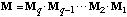
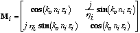
The characteristic matrix M for the Fabry-Perot cavity is given by
are the admittances of the environment
outside the sensor and of the medium from which the light comes, respectively.
The characteristic matrix M for the Fabry-Perot cavity is given by
 . (3)
. (3)
where Mi is the characteristic matrix of the optically homogenous
ith layer, with refractive index ni and thickness zi,
 (4)
(4)
with  [11].
[11].
Using the characteristic matrix method to analyze a multilayer system, for
example the spectral analysis of an optical filter, is easily done, but
the inverse problem (e.g., design of an optical filter which has arbitrary
spectral shape) is extremely difficult. For Fabry-Perot sensors, the gap
g must be inferred from some measurement of reflected light intensity I,
that is a function of the absolute reflectivity R, that is in turn
a function of wavelength and the structure of the sensor. It would be advantageous
if g could be directly expressed as a function of R and the thicknesses
zi of the other q - 1 layers, but for a general Fabry-Perot sensor
an analytic form for such an expression does not exist. One approach is
to find R as a function of g (assuming all the other layer thicknesses
are exactly known, using eqs. 1-4), and then use a fitting function gfit
to relate the gap g to the actual measurand I. This produces an error

 (5)
(5)
between the actual gap g and the fitted gap gfit.
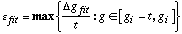
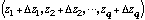
To choose a fitting function, the design space for the device must be specified.
Here we assume two primary design variables: i) the initial gap gi of the
Fabry-Perot cavity; and ii) the maximum mechanical travel t of the moving
mirror. The second variable is determined by the range of the sensed quantity
(e.g., the maximum pressure) and the mechanical compliance of the membrane
supporting the moving mirror. Since mechanical compliance frequently can
be adjusted independently of the thicknesses of the layers used to fabricated
the mirror, we will consider t a freely adjustable design variable. If we
wish to achieve the best accuracy [12] for a given initial gap gi and travel
t we must choose a fitting function so that the error 
 (6)
(6)
is minimized.
In addition to the simple errors due to response fitting, we should also
evaluate a particular design's tolerance to manufacturing errors; i.e.,
how errors propagate to g via process-induced uncertainties in the zi's.
In this case there exists an uncertainty [[Delta]]g in the gap at a given
reflected light intensity I since for mirror layers with thicknesses
 there can exist a gap thickness
  that would produce
an identical value of I
that would produce
an identical value of I
 (7)
(7)
where the functional dependencies of R have been indicated explicitly.
In principle, it should be possible to evaluate a given design by calculating
the response for all possible thickness combinations weighted by the distribution
functions representing the process-induced thickness variation of each layer.
This approach is computationally impractical when q becomes large (for instance,
if the cavity mirrors are made using multi-layer dielectric mirrors). Here
[[Delta]]g can be estimated efficiently provided that the first order Taylor
series approximation for I is valid
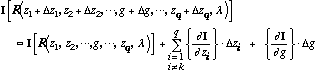 . (8)
. (8)
Combining eqs. 7 and 8 then gives [[Delta]]g; the maximum uncertainty [[Delta]]gproc
in gap due to process-induced thickness variations is
 . (9)
. (9)
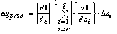
In terms of yield, if for each mirror layer i (i != k) the fraction
of devices with thickness between  and
and  is Pi, then for
a fixed value of I, the fraction of sensors
is Pi, then for
a fixed value of I, the fraction of sensors  with gap between
 and
and  that would produce this value of
 would be at least
 . (10)
To select a particular design, it is critical to remember that manufacturing
uncertainty in layer thicknesses also includes the process that determines
gi. Even if we assume a single calibration measurement is made to determine
the specific value of gi for a given manufactured sensor, the overall design
should still allow gi to vary over the range gi.(1 +/- d ),
where d is the normalized thickness uncertainty for the gap layer. For example,
if we wish to find the accuracy for a given nominal initial gap gi and travel
t, including the uncertainties induced by thickness variations in all the
layers, we must find the error 
 . (11)
The best design (i.e., the best values of gi and t) is the one that minimizes
. In terms of yield, if the fraction of sensors with
actual gap in the range gi.(1 +/- d ) is Pk, then
the fraction of sensors P with accuracy not worse than is at least
 . (12)
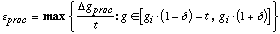
If both fitting and process-induced errors are included, to find the design
that would give the best accuracy we must find the combination of initial
gap gi and travel t so that the total error 
 (13)
(13)
is minimized.
To actually evaluate sensor errors the measurand I must be specified.
One possibility would be to attempt to directly measure the absolute reflectance
of the cavity at a single wavelength [[lambda]]1
 . (14)
This response curve will be periodic in g, with period [[lambda]]1/2. Unfortunately,
if there are any optical system losses, it is usually not possible to measure
the absolute value of reflectance, and hence g cannot be determined. An
alternative is the dual wavelength technique, in which relative reflected
intensities at two different wavelengths ([[lambda]]1 and [[lambda]]2) are
separately measured, and then a ratio is calculated using
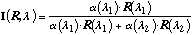 (15)
(15)
where  accounts for any losses induced by the optical system.
If over the wavelength range used these losses are wavelength independent
(such as bending loss or temperature-induced variations) the ratio given
by eq. 10 becomes equal to the corresponding ratio of absolute reflectances,
and so
accounts for any losses induced by the optical system.
If over the wavelength range used these losses are wavelength independent
(such as bending loss or temperature-induced variations) the ratio given
by eq. 10 becomes equal to the corresponding ratio of absolute reflectances,
and so
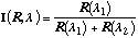 . (16)
This technique eliminates errors resulting from wavelength-independent changes
in the fiber interconnect to the sensor [1, 2, 4] . The response curve is
still a periodic function with respect to gap, but with a period equal to
the lowest common multiple of  and
and  .
.
Example Designs
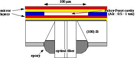
Typical experimental setup and micromachined Fabry-Perot sensors are shown
in [2, 4]. For simplicity, we consider a Fabry-Perot sensor whose moving
mirror is fabricated using a metal-coated, heavily boron-doped silicon membrane.
We assume the fixed mirror is metal-coated SiO2. Each metal mirror is assumed
to be made of a Au layer with nominal thickness of 70 Å. The thickness
of the silicon membrane is assumed to be much greater than the absorption
depth of the silicon at the wavelengths used. Thickness variation [[Delta]]z
for the metal layers is assumed to be  Å (three
sigma), which can be achieved with thin film coating equipment. The refractive
indexes for Au and silicon, as a function of wavelength, are obtained from
[13]. For the process used to set the initial gap, we assume a three sigma
uncertainty of 3 % (i.e., d = 0.03).
Å (three
sigma), which can be achieved with thin film coating equipment. The refractive
indexes for Au and silicon, as a function of wavelength, are obtained from
[13]. For the process used to set the initial gap, we assume a three sigma
uncertainty of 3 % (i.e., d = 0.03).
Figure 2 shows the calculated single wavelength absolute reflectance curve
(from eqs. 1-4), assuming [[lambda]]1 = 700 nm. The periodicity of the curve
suggests two basic operating branches, one between 1000 Å and 2750
Å, and the other between 2750 Å and 4500 Å. To illustrate
a design process, we first assume it is desirable to find a design that
produces the best accuracy when using a linear response approximation. Figure
3 shows the accuracy contour plot ( from eq. 6) over the
design space of gi and t. This shows, for instance, that 1 % accuracy could
be obtained from two designs, gi = 2625 Å and t = 375 Å,
or gi = 3450 Å and t = 375 Å, if there were no manufacturing
variations, and the only source of error was the linear fitting approximation.
For this device and wavelength choice, we have also calculated the process-induced
errors using eq. 9 (Fig. 2). For comparison, extensive random combinations
of Au mirror thicknesses from 67 Å to 73 Å have been tested
to verify that the maximum change in g is produced by the perturbed layer
thicknesses used in eq. 9. Agreement between the two approaches indicates
that the first order Taylor series approximation used in eq. 8 is sufficient
for this device. Figure 4 shows the error contours including both the manufacturing
layer thickness variations and the linear response fitting error (from eq.
13). In this case, the sensitivity to process variations is not the same
on the two branches of the response curve, and is much larger
than . The optimum design is now gi = 2600 Å and t =
325 Å, which will yield better than 5 % accuracy for at least 97 %
of the sensors manufactured.
Figure 5 shows the response curve and associated manufacturing-induced errors
for dual wavelength detection, assuming detection wavelengths of 560 nm
and 700 nm. There are now nine distinct operating branches. Calculation
of the contours of linearity error only (using eq. 6) indicates that an
accuracy not worse than 1 % could be achieved using gi = 6250 Å and
t = 1050 Å. Note that when using dual wavelength detection linearity
is maintained over a much longer travel than for single wavelength detection,
as has been noted in [4]. Consideration of process-induced errors only (from
eq. 11, using the full non-linear response curve as a reference) suggests
an optimum design for gi = 9325 Å and t = 825 Å, with at least
97 % of the sensors producing an accuracy of not worse than 1 %. Figure
6 shows the contour plot of the error induced by both linearity and layer
thickness variation for the branch with best performance. This shows that
when both errors are considered the optimum design is gi = 6050 Å
and t = 650 Å, with at least 97 % of the manufactured sensors producing
an accuracy of not worse than 3.5 %.
Conclusions
If Fabry-Perot-based sensors are to be manufactured in volume at low cost,
it will not be practical to individually calibrate every sensor to eliminate
fabrication-induced response variations. Here we have shown that variations
in the layer thicknesses used in such devices can contribute significantly
to errors, but that through proper design, high yield with reasonable accuracy
can still be achieved. For the specific example of a Fabry-Perot gap sensor
discussed here, even with 3 % (three sigma) layer thickness variations,
linear response with better than 5 % accuracy can be achieved from at least
97 % of the sensors by choosing the proper nominal initial gap and associated
maximum mechanical travel. The models and design methodology discussed can
also be extended easily to other sources of manufacturing variation, such
as dielectric constant fluctuation. Finally, it should be straightforward
to apply our approach to other interference-based micromachined devices,
such as tunable optical filters and modulators [14], to find designs that
minimize device sensitivity to process-induced variations.
Acknowledgments: This work was sponsored by the Advanced Research Projects
Agency (ARPA) Embedded Microsystems Program under contract # DABT63-92-C-0027
AMD P00002 - DOD-ARPA.
References
1. B. Halg, "A silicon pressure sensor with a low-cost contactless
interferometric optical readout," Sensors and Actuators A, vol.
30, pp. 225-229, 1992.
2. J. P. Dakin, C. A. Wade, and P. B. Withers, "An optical fiber pressure
sensor," SPIE Fiber optics '87: Fifth International Conference on
Fiber optics and Opto-electronics, 1987, pp. 194-201.
3. C. E. Lee and H. F. Taylor, "Fiber-optic Fabry-Perot Temperature
Sensor Using a Low-Coherence Light Source," Journal of Lightwave
Technology, vol. 9, pp. 129-134, 1991.
4. R. A. Wolthuis, G. L. Mitchell, E. Saaski, J. C. Hartl, and M. A. Afromowitz,
"Development of medical pressure and temperature sensors employing
optical spectrum modulation," IEEE Trans. on Biomedical Engin.,
vol. 38, pp. 974-980, 1991.
5. Y. Kim and D. P. Neikirk, "Monolithically Integrated Optically Interrogated
Pressure Microsensor," Journal of Acoustic Society of America, 124th
meeting, New Orleans, LA, 1992, pp. 2353.
6. H. A. Macleod, Thin-film optical filters. New York: McGraw-Hill,
1986.
7. H. A. Macleod, "Thin film narrow band optical filters," Thin
Solid Films, vol. 34, pp. 335-342, 1976.
8. P. Bousquet, A. Fornier, R. Kowalczyk, E. Pelletier, and P. Roche, "Optical
filters: monitoring process allowing the auto-correction of thickness errors,"
Thin Solid Films, vol. 13, pp. 285-290, 1972.
9. D. Gloge, "Weakly Guiding Fibers," Applied Optics, vol.
10, pp. 2252-2258, 1971.
10. D. Marcuse, "Loss Analysis of Single Mode Fiber Slices," The
Bell System Technical Journal, vol. 56, pp. 703-718, 1977.
11. M. Born and E. Wolf, Principles of Optics. Oxford: Pergamon Press,
1980.
12. L. Ristic, Ed., Sensor Technology and Devices. Boston: Artech
House, 1994.
13. E. D. Palik, Ed., Handbook of Optical Constants of Solids. Orlando,
FL: Academic Press, 1985.
14. K. W. Goossen, J. A. Walker, and S. C. Arney, "Silicon modulator
based on mechanically-active anti-reflection layer for fiber-in-the-loop
applications," Optical Fiber Communications, San Jose, CA, 1994,
pp. 50.
Optically interrogated Fabry-Perot pressure sensor.
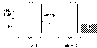
Figure 1: Schematic diagram of multilayer Fabry-Perot sensor. The device
consists of q layers, where layers 1 through k - 1 make up the
"moving" mirror, layer k is the gap to be measured, and layers
k + 1 through q make up the "fixed" mirror. Each mirror
layer i is zi thick, with manufacturing-induced thickness error [[Delta]]zi.
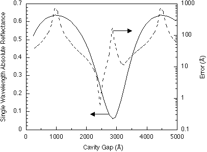
Figure 2: Solid line: absolute reflectance (single wavelength response curve,
eq. 14, [[lambda]]1 = 700 nm) versus gap for Fabry-Perot cavity described
in the text. Dashed line: process-induced response variations (from eq.
9).
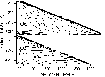
Figure 3: Accuracy contour map for single wavelength detection as a function
of initial gap and mechanical travel, assuming the only errors are those
produced by using a linear response approximation.
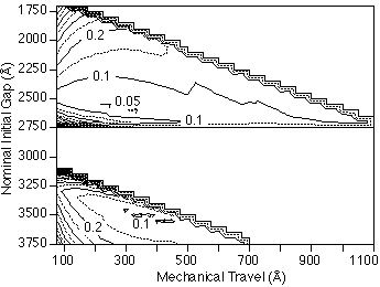
Figure 4: Accuracy contour map for single wavelength detection, assuming
both process-induced variations and linear response errors. Optimum performance
occurs for gi = 2600 Å and t = 325 Å, which will yield better
than 5 % accuracy for at least 97 % of the sensors manufactured.
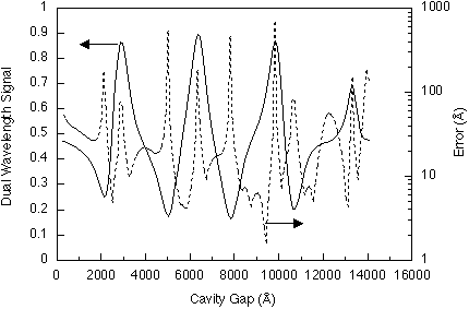
Figure 5: Solid line: dual wavelength response curve (from eq. 16, [[lambda]]1
= 560 nm and [[lambda]]2 = 700 nm) versus gap for Fabry-Perot cavity described
in the text. Dashed line: process-induced response variations (from eq.
9). The period of the response function is 14,000 Å, containing nine
distinct branches.
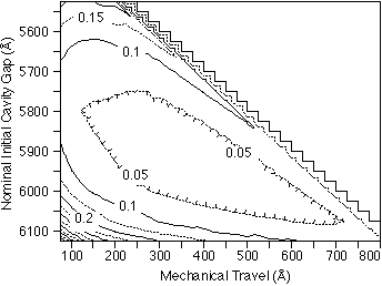
Figure 6: Accuracy contour map for due wavelength detection, assuming both
process-induced variations and linear response errors. Optimum performance
occurs for gi = 6050 Å and t = 650 Å, with at least 97 % of
the manufactured sensors producing an accuracy of not worse than 3.5 %.