
Conductor Loss Calculation of V-shaped Conductor-Backed Coplanar Waveguide
B.-T. Lee and D. P. Neikirk
Department of Electrical and Computer Engineering
Electrical Engineering Research Laboratory
The University of Texas at Austin
Austin, Texas 78712
Abstract
Recently it has been proposed that ohmic conductor loss in coplanar waveguide can be reduced by using a V-shaped ground plane backing. Here we calculate the conductor loss for constant 50 [Omega] characteristic impedance designs. Several different techniques of varying numerical efficiency for evaluating the loss have also been compared.
Introduction
Recently a new type of conductor-backed coplanar waveguide [1] has been proposed, where the back side ground plane is made V-shaped in order to reduce current crowding and conductor loss, as illustrated in Fig. 1. However, no accurate models for the actual conductor loss in these structures have been reported. Typically, for conductor loss evaluation methods such as the incremental inductance rule [2], integration over surface current distribution [3], etc., have been used. When the metal thickness is on the order of the skin-depth, the incremental inductance rule gives poor results, and rigorous full-wave solvers are numerically expensive. To efficiently and accurately capture transmission line resistance and inductance from dc to high frequencies an effective internal impedance approach can be used, coupled with an external field solver. Here we apply both a conformal mapping technique [4] and a more accurate current ribbon technique [5] to evaluate the conductor loss in V-groove conductor-backed coplanar waveguide (VGCPW). For constant characteristic impedance designs, the VGCPW does show some reduction in loss at high frequencies, and for design purposes, conformal mapping-based models have been found to be reasonably accurate, as well as numerically efficient.
Surface Ribbon Method for Series Impedance Calculation
In the volume filament method (VFM) [6], each conductor of a transmission line structure is divided into many small filaments, with uniform current density assumed across each of the small filaments. The amount of current does vary from filament to filament to properly capture skin and proximity effects. The dc resistance and self-inductance of each filament and the mutual inductances between all filaments are used to construct an inductance matrix, and from this the series impedance for the transmission line is computed. This method gives accurate ac resistance and inductance for quasi-TEM transmission lines. However at the frequencies where the skin-effect is dominant, the filament dimensions must be quite small, and large, dense matrices lead to long computation time.
For greater numerical efficiency it has been shown that the internal characteristics of the conductors can be accurately modeled using an effective internal impedance (EII) representing resistance and internal inductance of the conductor, and volume filaments replaced by surface ribbons [5]. This surface ribbon method (SRM) considerably reduces the matrix size and computational load without loss in accuracy.
Conformal Mapping Technique in conjunction with Effective Internal Impedance
Frequency-dependent resistance and inductance can also be approximated using conformal mapping [4]. The original polygonal geometry of the transmission line is transformed into parallel plates through a sequence of two Schwarz-Christoffel transformations, and the surfaces of the conductors are represented by the EII, scaled into the mapped domain. The series impedance per length of a transmission line first requires the determination of the Schwarz-Christoffel mapping coefficients, followed by an integration to compute the series impedance. The latter procedure is a trivial process, so this method is very efficient once the mapping coefficients have been obtained.
Results for V-Groove Conductor-backed Coplanar Waveguide (VGCPW)
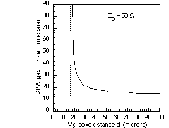
To determine if the V-groove reduces loss, design constraints must first be set. Since the center conductor contributes the most to loss we chose to hold the center conductor width fixed. The location of the CPW ground plane (i.e., b) for a specified V-groove depth (i.e., d and h are given) is determined to maintain a high frequency characteristic impedance of 50 [Omega]. To compute the characteristic impedance, capacitance is calculated using a conformal mapping technique by assuming the air-dielectric boundary is a perfect magnetic wall. We have also compared this result to the boundary element method (BEM); the conformal map result including the thickness of the CPW metal agreed with BEM results to within a few percent up to the fairly wide gap (b - a) of 90 um. Figure 1 shows the resulting gap (b - a) necessary to maintain 50 [Omega] impedance as a function of the V-groove separation d. Figure 2 compares the resistance and loss per unit length calculated with the different methods for a simple conductor-backed CPW (d = h = 100 um). Figure 3 compares the resistance and loss per unit length for a 50 [Omega] VGCPW with 20 um wide center conductor (a = 10 um, b = 50 um, d = 20 um, h = 100 um). As the V-groove gets closer to the center conductor than 20 um the CPW ground plane gap rapidly increases to infinity, i.e., to maintain 50 [Omega] characteristic impedance the structure becomes a pure V-groove microstrip line. All methods are in good agreement, although the conformal map including metal thickness slightly over estimates the loss. The surface ribbon method is almost identical to the volume filament method, but is much faster (Table I). Figure 4 shows a comparison of the resistance and loss for different 50 [Omega] designs, ranging from pure CPW, to pure V-groove microstrip, to a simple microstrip with substrate thickness chosen to give 50 [Omega] impedance. The high frequency resistance does decrease as the V-groove gap d decreases and CPW gap (b - a) increases, eventually approaching that of the simple microstrip line (which here was the minimum loss configuration). For example, at 46.4 GHz the calculated attenuation constant is 2.5 dB/cm for the normal CPW, falling to 2.26 dB/cm for VGCPW with b - a = 21 um and d = 31 um, or 2.16 dB/cm for b - a = 40 um and d = 20 um; for comparison, the calculated loss for simple 50 [Omega] microstrip (20 um wide strip, 26 um thick high resistivity Si substrate) was 2.07 dB/cm.
Conclusions
To efficiently and accurately capture transmission line resistance and inductance from dc to high frequencies we have applied both conformal mapping techniques and a more accurate current ribbon method to V-groove conductor-backed coplanar waveguide (VGCPW). For design purposes, conformal mapping-based models are reasonably accurate, as well as numerically efficient. For constant characteristic impedance designs, the VGCPW does show some reduction in loss at high frequencies, although the rather small reduction may not justify the added complexity of fabrication.
This work was sponsored in part by the Advanced Research Projects Agency Application Specific Electronic Module program and the Texas Advanced Technology Program.
References
[1] K.-K. M. Cheng and I. D. Robertson, "Quasi-TEM Analysis of V-Shaped Conductor-Backed Coplanar Waveguide," IEEE Transactions on Microwave Theory and Techniques, vol. 43, pp. 1992-1994, 1995.
[2] H. A. Wheeler, "Formulas for the skin-effect," Proceedings of the Institute of Radio Engineers, vol. 30, pp. 412-424, 1942.
[3] R. E. Collin, Foundations for Microwave Engineering, 2nd ed. New York: McGraw-Hill, 1992.
[4] E. Tuncer, B.-T. Lee, M. S. Islam, and D. P. Neikirk, "Quasi-Static Conductor Loss Calculations in Transmission Lines using a New Conformal Mapping Technique," IEEE Transactions on Microwave Theory and Techniques, vol. 42, pp. 1807-1815, 1994.
[5] E. Tuncer, B.-T. Lee, and D. P. Neikirk, "Interconnect Series Impedance Determination Using a Surface Ribbon Method," IEEE 3rd Topical Meeting on Electrical Performance of Electronic Packaging, Monterey, CA, Nov. 2-4, 1994, pp. 249-252.
[6] W. T. Weeks, L. L. Wu, M. F. McAllister, and A. Singh, "Resistive and inductive skin effect in rectangular conductors," IBM Journal of Research and Development, vol. 23, pp. 652-660, 1979.
[7] H. Wheeler, "Transmission-Line Properties of a Strip on a Dielectric Sheet on a Plane," IEEE Transactions on Microwave Theory and Techniques, vol. MTT-25, pp. 631-647, 1977.
(a)
(b)
Figure 1: (a) V-shaped conductor-backed coplanar waveguide (VGCPW); the angle corresponds to an anisotropically etched groove in (100) Si. (b) CPW gap (b - a) as a function of the V-groove distance d for a constant Zo = 50 [Omega] design; dotted line : distance d = 16 um for a 50 [Omega] V-groove microstrip line (i.e., no CPW ground planes).
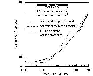
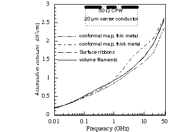
Figure 2: Comparison of various modeling techniques for conductor loss of a 50 [Omega] CPW with 20 um wide center conductor (a = 10 um, b = 25 um, d = h = 100 um). The volume filament method (VFM) is the most exact, but least numerically efficient; the surface ribbon method (SRM) is nearly identical to the VFM, but about sixty times faster; the thin metal conformal map approximation is fairly accurate, and somewhat faster than the SRM.
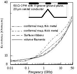
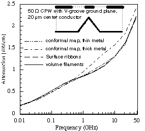
Figure 3: Comparison of various modeling techniques for conductor loss of a 50 [Omega] VGCPW with 20 um wide center conductor (a = 10 um, b = 50 um, d = 20 um, h = 100 um). For this groove depth the structure is almost a pure V-groove microstrip line.
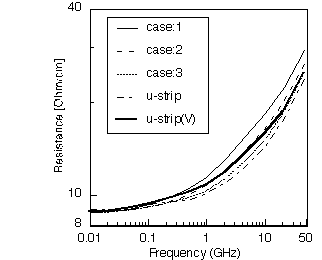
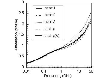
Figure 4. Comparison of several 50 [Omega] designs: case 1: b - a = 15 um, d = 100 um (normal CPW); case 2: b - a = 21 um, d = 31 um; case 3: b - a = 40 um, d = 20 um; case 4: 50 [Omega] microstrip line designed using reference [7], w = 20 um, h = 26 um; case 5: 50 [Omega] microstrip line with V-shaped ground plane, 2a = 20 um, d = 16 um, b - a = [infinity].
| Transmission | Method | Number of | CPU time (sec) | |
| Line Structure | unknowns | pre-process | solve (per frequency) | |
| VGCPW, | "thin metal" CM | 2 | 8.6 | 0.15 |
| microstrip | "thick metal" CM | 6 | 8.6 | 0.15 |
| VGCPW | VFM | 1009 | 300 | 350 |
| SRM | 265 | 3 | 7 | |
| microstrip | VFM | 599 | 35 | 75 |
| SRM | 165 | 1.4 | 1.8 |