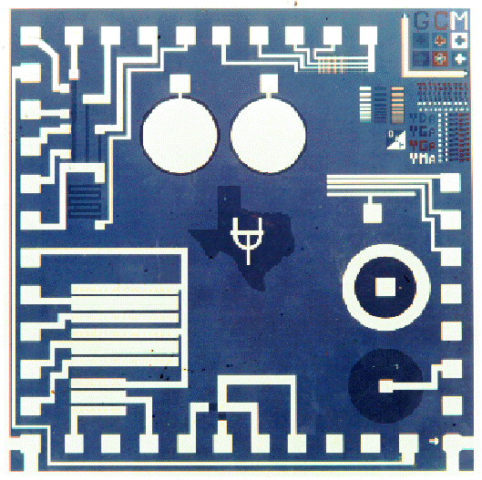
This section describes in detail the functions of the Holberg Mask
Set, shown with all four layers overlaid in Fig. 1, p. 38, and level-by-level
in Fig 2a-2d, pp. 39-42. Each functional block on the chip is discussed
separately. These blocks are:
i) Alignment, resolution, and registration patterns
ii) Metal step coverage and leakage patterns
iii) Diffused resistor and contact resistance test structures
iv) Diffused diodes
v) MOS capacitors
vi) Thick and thin oxide MOSFETs
Alignment, resolution, and registration patterns
The purpose of this part of the chip is to allow accurate alignment
of each mask level to preceding levels already patterned, as well as to
evaluate the accuracy of the alignment and the resolution of both lithographic
and etching processes. The area in the upper right corner of the chip (Fig.
1) is used for these purposes, and is shown level by level in Fig. 2a-2d.
Figure 3 (p. 43) shows a 200x, four level composite view of this region
of the chip.
Figure 4 (pp. 44-45) shows a diagram to illustrate how the registration
verniers are used to determine mis-alignment. In Mask Level 1 (Diffusion,
Fig. 2a) windows are opened to provide the center part of the verniers;
each subsequent level patterns bars on either side of the Level 1 pattern.
Misalignment is determined by finding the outer and inner boxes which line
up, and counting how many boxes from the end this occurs at. Each box from
the end corresponds to 1 um misregistration.
Diffused resistor and contact resistance test structures
The purpose of this part of the chip is to allow us to measure the sheet
resistance due to our diffusions, as well as to find contact and bend resistance
corrections. The area in the upper left corner of the chip (Fig. 1) is used
for these purposes, and is shown level by level in Fig. 2a-2d. Figure 5
(p. 46) shows a 100x, three level composite (diffusion: Level 1; contact:
Level 3; and metal: Level 4) view of this region of the chip.
There are four basic structures in this region. Two straight resistors,
one short (R1) and one long (R2), are used to find sheet and contact resistances.
Another serpentine resistor (R3) is used to find the equivalent size and
resistance of bends. The last structure allows four point measurement of
sheet resistance, to help remove contact resistance problems from the measurements.
See the TEST section, p. 31 for more details.
Diffused diodes
The purpose of this part of the chip is to allow us to evaluate a diffused
p-n junction diode. The region in the lower right corner of the chip (Fig.
1) is used for this purpose, and is shown level by level in Fig. 2a-2d.
There are two diodes of identical size, the top device also having a field
relief plate over the oxide covering the surface p-n junction.
MOS capacitors
The purpose of this part of the chip is to allow us to evaluate the
quality of our gate oxides. The region in the upper center of the chip (Fig.
1) is used to make two MOS capacitors at the same time we grow the gate
oxide for our MOSFETs. This area is also shown level by level in Fig. 2a-2d.
There are two capacitors of equal metal plate and thin oxide areas. The
right device, however, also has a diffused guard ring around the perimeter
of the capacitor.
Thick and thin oxide MOSFETs
The purpose of this part of the chip is fabricate two MOSFETs with different
gate lengths, as well as a thick oxide MOSFET to help evaluate the quality
of our field oxide. The area in the bottom left corner of the chip (Fig.
1) is used for these purposes, and is shown level by level in Fig. 2a-2d.
Figure 6 (p. 47) shows a 100x, four level composite view of this region
of the chip. The upper MOSFET (Device 1) has a longer channel than the device
below it (Device 2). All three MOSFETs share a common source connection
through the upper-most pad shown in Fig. 6.
Critical Mask Dimensions:
MOSFET channels:
Device 1 800um x 30um
Device 2 800um x 20um
MOS cap w guard ring: 600um diam.
MOS cap w/o guard ring: 550um diam.
Diode diffusion diam.: 550um
Diffused resistors (straight):
Device 1 250um (l) x 25um (w)
Device 2 500um (l) x 25um (w)
Registration verniers: 1um increments
Resolution bars:
   line     line         following           line     line        following
  number                   space            number                space
    1          2 um     2 um
    2          2 um     3 um                  8       10 um       10 um
    3          3 um     3 um                  9       15 um       15 um
    4          3 um     5 um                  10      15 um       15 um
    5          5 um     5 um                  11      20 um       20 um
    6          5 um     5 um                  12      20 um       20 um
    7         10 um     10 um                 13      25 um       25 um
                                              14      25 um
Contact Windows:
Diffusion area: 50um x 50um
Oxide window size (metal/semiconductor contact area):
25um x 25um
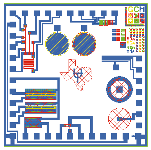
Figure 1: Composite drawing of the Holberg Mask set.
Figure 2a: Holberg Mask Level 1, Diffusion
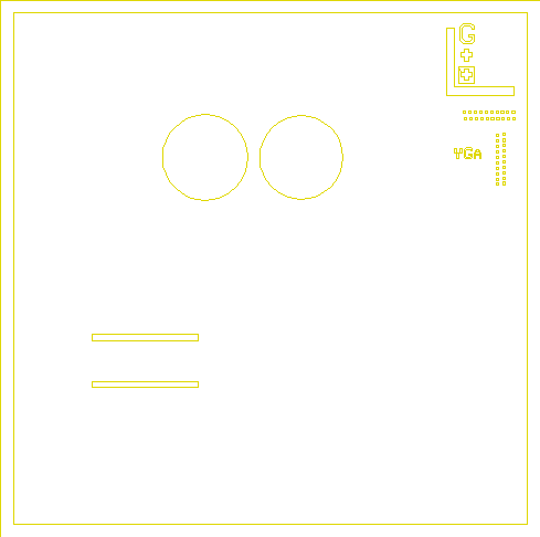
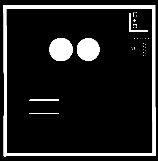
Figure 2b: Holberg Mask Level 2, Gate
Figure 2c: Holberg Mask Level 3, Contacts
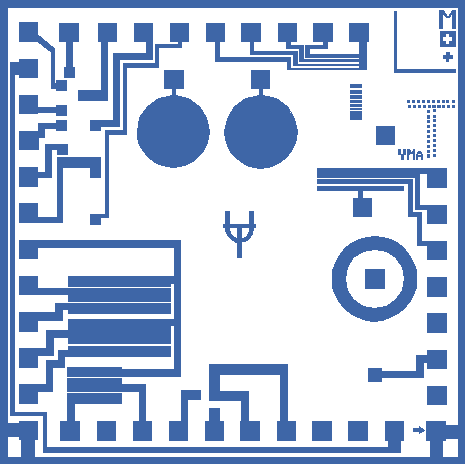
Figure 2d: Holberg Mask Level 4, Metal

Figure 3: Composite view of alignment and registration patterns of Holberg
Mask Set; all four levels are shown superimposed. The scale bar is 50 um
long.

Figure 4a: Illustration of y-axis misregistration verniers. Three
cases are shown: zero, +1, and -1 um misregistration.
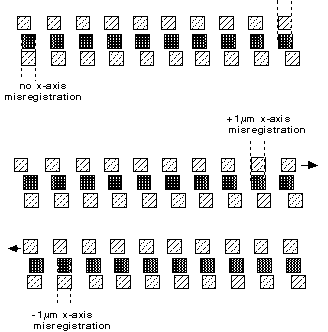
Figure 4b: Illustration of x-axis misregistration verniers. Three cases are shown: zero, +1, and -1 um misregistration.

Figure : Resolution test pattern.
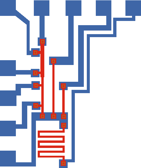
Figure 5: Composite view of resistor patterns of Holberg Mask Set; three
levels are shown superimposed: diffusion: Level 1; contact: Level 3; and
metal: Level 4. The scale bar is 100 um long.
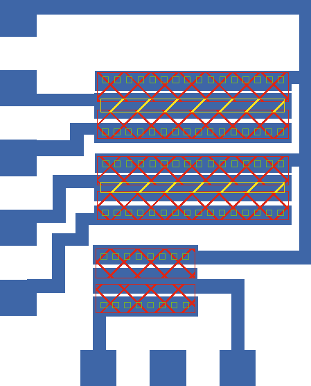
Figure 6: Composite view of MOSFET patterns of Holberg Mask Set; all four
levels are shown superimposed. The scale bar is 100 um long.